Vishay SIHK Type N-Channel MOSFET, 19 A, 600 V Enhancement, 8-Pin PowerPAK 10 x 12 SIHK155N60E-T1-GE3
- RS Stock No.:
- 279-9920
- หมายเลขชิ้นส่วนของผู้ผลิต / Mfr. Part No.:
- SIHK155N60E-T1-GE3
- ผู้ผลิต:
- Vishay

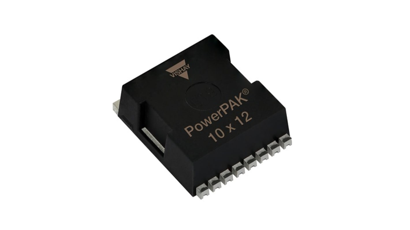
รูปภาพประกอบสินค้าเป็นเพียงรูปภาพใกล้เคียงเท่านั้น กรุณาอ่านรายละเอียดสินค้า
มีส่วนลดเมื่อซื้อจำนวนมาก
ดูตัวเลือกการกำหนดราคาในการซื้อปริมาณมากยอดรวมย่อย (1 ชิ้น)*
THB158.94
(ไม่รวมภาษีมูลค่าเพิ่ม)
THB170.07
(รวมภาษีมูลค่าเพิ่ม)
ส่งฟรีหากซื้อเกิน ฿2,500.00
มีในสต็อก
- 2,000 ชิ้นพร้อมจัดส่งจากคลังสินค้าต่างประเทศ
ต้องการสินค้าเพิ่มหรือไม่ ระบุจำนวนและคลิก ‘ตรวจสอบวันจัดส่ง’ เพื่อดูข้อมูลเพิ่มเติมเกี่ยวกับสต็อกสินค้าและการจัดส่ง
ชิ้น | ต่อหน่วย |
|---|---|
| 1 - 49 | THB158.94 |
| 50 - 99 | THB155.81 |
| 100 - 249 | THB152.68 |
| 250 - 999 | THB149.55 |
| 1000 + | THB146.41 |
*ตัวบ่งบอกราคา / price indicative
- RS Stock No.:
- 279-9920
- หมายเลขชิ้นส่วนของผู้ผลิต / Mfr. Part No.:
- SIHK155N60E-T1-GE3
- ผู้ผลิต:
- Vishay
คุณสมบัติ / Specifications
ข้อมูลทางเทคนิค / Technical Data Sheets
Legislation and Compliance
รายละเอียดสินค้า / Product Details
ค้นหาผลิตภัณฑ์ที่คล้ายกันโดยเลือกคุณลักษณะอย่างน้อยหนึ่งรายการ
เลือกทั้งหมด | คุณลักษณะ | ค่า |
|---|---|---|
| Brand | Vishay | |
| Product Type | MOSFET | |
| Channel Type | Type N | |
| Maximum Continuous Drain Current Id | 19A | |
| Maximum Drain Source Voltage Vds | 600V | |
| Package Type | PowerPAK 10 x 12 | |
| Series | SIHK | |
| Mount Type | Surface | |
| Pin Count | 8 | |
| Maximum Drain Source Resistance Rds | 0.158Ω | |
| Channel Mode | Enhancement | |
| Typical Gate Charge Qg @ Vgs | 36nC | |
| Minimum Operating Temperature | -55°C | |
| Maximum Power Dissipation Pd | 156W | |
| Forward Voltage Vf | 1.2V | |
| Maximum Gate Source Voltage Vgs | 30V | |
| Maximum Operating Temperature | 150°C | |
| Standards/Approvals | RoHS | |
| Length | 9.9mm | |
| Automotive Standard | No | |
| เลือกทั้งหมด | ||
|---|---|---|
Brand Vishay | ||
Product Type MOSFET | ||
Channel Type Type N | ||
Maximum Continuous Drain Current Id 19A | ||
Maximum Drain Source Voltage Vds 600V | ||
Package Type PowerPAK 10 x 12 | ||
Series SIHK | ||
Mount Type Surface | ||
Pin Count 8 | ||
Maximum Drain Source Resistance Rds 0.158Ω | ||
Channel Mode Enhancement | ||
Typical Gate Charge Qg @ Vgs 36nC | ||
Minimum Operating Temperature -55°C | ||
Maximum Power Dissipation Pd 156W | ||
Forward Voltage Vf 1.2V | ||
Maximum Gate Source Voltage Vgs 30V | ||
Maximum Operating Temperature 150°C | ||
Standards/Approvals RoHS | ||
Length 9.9mm | ||
Automotive Standard No | ||
Vishay SIHK Series MOSFET, 600V Drain Source Voltage, 19A Continuous Drain Current - SIHK155N60E-T1-GE3
This MOSFET is a high-voltage enhancement-mode N-channel switching transistor designed for surface-mount power conversion and control applications. It suits circuits requiring robust drain-to-source blocking at elevated voltages while operating across a wide temperature span.
Features and Benefits:
• 600V drain-source rating enables high-voltage designs • 19A continuous drain current supports substantial load currents • 0.158Ω Rds(on) reduces conduction losses during operation • 36nC typical gate charge for predictable switching performance • 156W power dissipation allows sustained heat handling • 150°C maximum operating temperature tolerates elevated thermal stress
Applications
• Suitable for offline SMPS primary switches in power supplies • Ideal for industrial motor drive switching stages • Used for high-voltage DC-DC converters in automation systems • Can be used for inverter output stage switching in electrical drives • Used for switch-mode loads in mechanical control equipment
What package should I account for when laying out the board?
The device is supplied in an 8-pin PowerPAK10x12 surface-mount package, requiring a footprint compatible with that thermal pad and lead arrangement.
What gate voltage range is safe for control circuitry?
The maximum permissible gate-to-source voltage is 30V, so driver circuits should retain gate excursions within that limit.
How does it behave thermally under load?
It can dissipate up to 156W
thermal management must ensure junction-to-ambient temperature stays within limits for reliable operation up to its 150°C rating.
Are there environmental or regulatory design considerations?
It is RoHS-compliant, allowing use in designs that restrict hazardous substances.
What switching characteristic affects driver selection?
The typical gate charge is 36nC at the rated gate voltage, which determines the required drive current and switching speed trade-offs.
ลิงก์ที่เกี่ยวข้อง
- Vishay SIHK Type N-Channel MOSFET 600 V Enhancement, 8-Pin PowerPAK 10 x 12 SIHK155N60E-T1-GE3
- Vishay SIHK Type N-Channel MOSFET 650 V Enhancement, 8-Pin PowerPAK 10 x 12 SIHK105N60E-T1-GE3
- Vishay SIHK Type N-Channel MOSFET 650 V Enhancement, 8-Pin PowerPAK 10 x 12 SIHK185N60EF-T1GE3
- Vishay SIHK Type N-Channel MOSFET 650 V Enhancement, 8-Pin PowerPAK 10 x 12 SIHK105N60EF-T1GE3
- Vishay SIHK Type N-Channel MOSFET 650 V Enhancement, 8-Pin PowerPAK 10 x 12 SIHK045N60EF-T1GE3
- Vishay SIHK Type N-Channel MOSFET 650 V Enhancement, 8-Pin PowerPAK 10 x 12 SIHK125N60EF-T1GE3
- Vishay SIHK Type N-Channel MOSFET 600 V Enhancement, 8-Pin PowerPAK 10 x 12 SIHK155N60EF-T1GE3
- Vishay SIHK Type N-Channel MOSFET 650 V Enhancement, 8-Pin PowerPAK 10 x 12 SIHK085N60EF-T1GE3