Vishay SISS5208DN Type N-Channel Single MOSFETs, 172 A, 20 V Enhancement, 8-Pin PowerPAK SISS5208DN-T1-GE3
- RS Stock No.:
- 653-148
- หมายเลขชิ้นส่วนของผู้ผลิต / Mfr. Part No.:
- SISS5208DN-T1-GE3
- ผู้ผลิต:
- Vishay

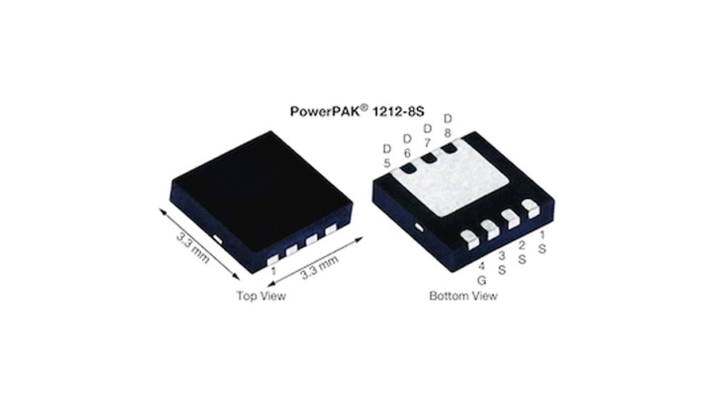
รูปภาพประกอบสินค้าเป็นเพียงรูปภาพใกล้เคียงเท่านั้น กรุณาอ่านรายละเอียดสินค้า
ยอดรวมย่อย (1 รีล รีลละ 3000 ชิ้น)*
THB77,382.00
(ไม่รวมภาษีมูลค่าเพิ่ม)
THB82,800.00
(รวมภาษีมูลค่าเพิ่ม)
ไม่สามารถเข้าถึงข้อมูลสต็อกได้ในขณะนี้ - โปรดกลับมาตรวจสอบอีกครั้งภายหลัง
ชิ้น | ต่อหน่วย | ต่อม้วน* |
|---|---|---|
| 3000 + | THB25.794 | THB77,382.00 |
*ตัวบ่งบอกราคา / price indicative
- RS Stock No.:
- 653-148
- หมายเลขชิ้นส่วนของผู้ผลิต / Mfr. Part No.:
- SISS5208DN-T1-GE3
- ผู้ผลิต:
- Vishay
คุณสมบัติ / Specifications
ข้อมูลทางเทคนิค / Technical Data Sheets
Legislation and Compliance
รายละเอียดสินค้า / Product Details
ค้นหาผลิตภัณฑ์ที่คล้ายกันโดยเลือกคุณลักษณะอย่างน้อยหนึ่งรายการ
เลือกทั้งหมด | คุณลักษณะ | ค่า |
|---|---|---|
| Brand | Vishay | |
| Channel Type | Type N | |
| Product Type | Single MOSFETs | |
| Maximum Continuous Drain Current Id | 172A | |
| Maximum Drain Source Voltage Vds | 20V | |
| Series | SISS5208DN | |
| Package Type | PowerPAK | |
| Mount Type | Surface | |
| Pin Count | 8 | |
| Maximum Drain Source Resistance Rds | 0.0013Ω | |
| Channel Mode | Enhancement | |
| Maximum Gate Source Voltage Vgs | 8V | |
| Minimum Operating Temperature | -55°C | |
| Maximum Power Dissipation Pd | 56.8W | |
| Typical Gate Charge Qg @ Vgs | 24.6nC | |
| Forward Voltage Vf | 1.1V | |
| Maximum Operating Temperature | 150°C | |
| Length | 3.40mm | |
| Height | 0.83mm | |
| Standards/Approvals | RoHS | |
| Width | 3.40mm | |
| Automotive Standard | No | |
| เลือกทั้งหมด | ||
|---|---|---|
Brand Vishay | ||
Channel Type Type N | ||
Product Type Single MOSFETs | ||
Maximum Continuous Drain Current Id 172A | ||
Maximum Drain Source Voltage Vds 20V | ||
Series SISS5208DN | ||
Package Type PowerPAK | ||
Mount Type Surface | ||
Pin Count 8 | ||
Maximum Drain Source Resistance Rds 0.0013Ω | ||
Channel Mode Enhancement | ||
Maximum Gate Source Voltage Vgs 8V | ||
Minimum Operating Temperature -55°C | ||
Maximum Power Dissipation Pd 56.8W | ||
Typical Gate Charge Qg @ Vgs 24.6nC | ||
Forward Voltage Vf 1.1V | ||
Maximum Operating Temperature 150°C | ||
Length 3.40mm | ||
Height 0.83mm | ||
Standards/Approvals RoHS | ||
Width 3.40mm | ||
Automotive Standard No | ||
- COO (Country of Origin):
- CN
Vishay SISS5208DN Series Single MOSFETs, 20V Maximum Drain Source Voltage, 172A Maximum Continuous Drain Current - SISS5208DN-T1-GE3
This single MOSFET is a surface-mount N-channel enhancement device designed for high-current switching in Compact power assemblies. It operates across a wide temperature range and is intended for applications requiring fast switching and substantial continuous drain capability while maintaining efficient thermal behaviour.
Features and Benefits:
• 172A continuous drain current enables high-load handling • 20V drain-source rating supports low-voltage power rails • 0.0013Ω Rds(on) reduces conduction losses • 24.6nC gate charge allows controlled switching dynamics • 56.8W power dissipation manages thermal stress under load • 150°C maximum operating temperature permits elevated environment use
Applications
• Suitable for motor drive stages in automation equipment • Ideal for high-current DC-DC converters in power supplies • Used for load switching in industrial control panels • Can be used for H-bridge output stages in robotics • Used with high-power MOSFET arrays in inverter modules
What gate voltage range should I plan for in gate-driver design?
The device accepts gate-source voltages up to 8V, so a gate driver that provides Vgs within this limit will ensure safe operation.
How does the package affect PCB layout and thermal paths?
The PowerPAK surface-mount package concentrates thermal and electrical connections on a small footprint, so copper pours and thermal vias are recommended to dissipate the device’s 56.8W power loss.
What ambient conditions are permissible for reliable operation?
The component is rated to operate down to -55°C and up to 150°C, allowing use across harsh industrial temperature ranges.
How should inrush or transient currents be considered in design?
With a low Rds(on) of 0.0013Ω and high continuous current capacity, transient stress should be assessed against surge capabilities and PCB trace current ratings to prevent overstress.
ลิงก์ที่เกี่ยวข้อง
- Vishay SISS5208DN Type N-Channel Single MOSFETs 20 V Enhancement, 8-Pin PowerPAK
- Vishay SIS9122 Dual N-Channel Single MOSFETs 100 V Enhancement, 8-Pin PowerPAK
- Vishay SIS5712DN Type N-Channel Single MOSFETs 150 V Enhancement, 8-Pin PowerPAK
- Vishay SIRA18DDP Type N-Channel Single MOSFETs 30 V Enhancement, 8-Pin PowerPAK
- Vishay SIS9122 Dual N-Channel Single MOSFETs 100 V Enhancement, 8-Pin PowerPAK SIS9122DN-T1-GE3
- Vishay SIS4406DN Type N-Channel Single MOSFETs 40 V Enhancement, 8-Pin PowerPAK
- Vishay SIR5712DP Type N-Channel Single MOSFETs 150 V Enhancement, 8-Pin PowerPAK
- Vishay SIR4406DP Type N-Channel Single MOSFETs 40 V Enhancement, 8-Pin PowerPAK