Vishay Dual TrenchFET 2 Type N-Channel MOSFET, 4.5 A, 20 V Enhancement, 8-Pin SC-70
- RS Stock No.:
- 228-2834
- หมายเลขชิ้นส่วนของผู้ผลิต / Mfr. Part No.:
- SIA938DJT-T1-GE3
- ผู้ผลิต:
- Vishay

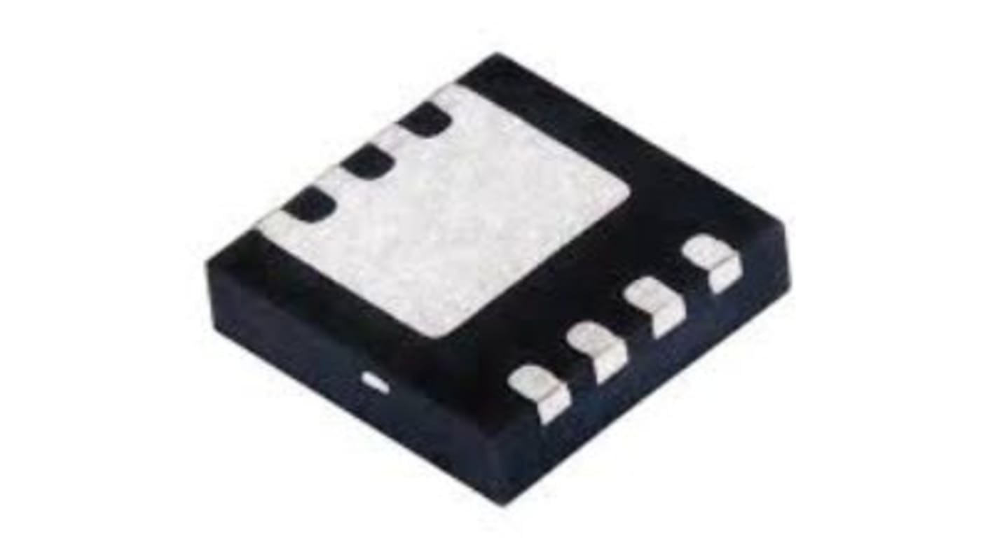
รูปภาพประกอบสินค้าเป็นเพียงรูปภาพใกล้เคียงเท่านั้น กรุณาอ่านรายละเอียดสินค้า
ยอดรวมย่อย (1 รีล รีลละ 3000 ชิ้น)*
THB26,904.00
(ไม่รวมภาษีมูลค่าเพิ่ม)
THB28,788.00
(รวมภาษีมูลค่าเพิ่ม)
ส่งฟรีหากซื้อเกิน ฿2,500.00
มีในสต็อก
- เพิ่มอีก 3,000 ชิ้นจะส่งได้หลังจากวันที่ 13 กรกฎาคม 2569 ไปอีกประมาณ 7 วันทำการ
ต้องการสินค้าเพิ่มหรือไม่ ระบุจำนวนและคลิก ‘ตรวจสอบวันจัดส่ง’ เพื่อดูข้อมูลเพิ่มเติมเกี่ยวกับสต็อกสินค้าและการจัดส่ง
ชิ้น | ต่อหน่วย | ต่อม้วน* |
|---|---|---|
| 3000 + | THB8.968 | THB26,904.00 |
*ตัวบ่งบอกราคา / price indicative
- RS Stock No.:
- 228-2834
- หมายเลขชิ้นส่วนของผู้ผลิต / Mfr. Part No.:
- SIA938DJT-T1-GE3
- ผู้ผลิต:
- Vishay
คุณสมบัติ / Specifications
ข้อมูลทางเทคนิค / Technical Data Sheets
Legislation and Compliance
รายละเอียดสินค้า / Product Details
ค้นหาผลิตภัณฑ์ที่คล้ายกันโดยเลือกคุณลักษณะอย่างน้อยหนึ่งรายการ
เลือกทั้งหมด | คุณลักษณะ | ค่า |
|---|---|---|
| Brand | Vishay | |
| Product Type | MOSFET | |
| Channel Type | Type N | |
| Maximum Continuous Drain Current Id | 4.5A | |
| Maximum Drain Source Voltage Vds | 20V | |
| Series | TrenchFET | |
| Package Type | SC-70 | |
| Mount Type | Surface | |
| Pin Count | 8 | |
| Maximum Drain Source Resistance Rds | 21.5mΩ | |
| Channel Mode | Enhancement | |
| Typical Gate Charge Qg @ Vgs | 3.5nC | |
| Minimum Operating Temperature | -55°C | |
| Maximum Power Dissipation Pd | 7.8W | |
| Transistor Configuration | Dual | |
| Maximum Operating Temperature | 150°C | |
| Standards/Approvals | No | |
| Number of Elements per Chip | 2 | |
| Automotive Standard | No | |
| เลือกทั้งหมด | ||
|---|---|---|
Brand Vishay | ||
Product Type MOSFET | ||
Channel Type Type N | ||
Maximum Continuous Drain Current Id 4.5A | ||
Maximum Drain Source Voltage Vds 20V | ||
Series TrenchFET | ||
Package Type SC-70 | ||
Mount Type Surface | ||
Pin Count 8 | ||
Maximum Drain Source Resistance Rds 21.5mΩ | ||
Channel Mode Enhancement | ||
Typical Gate Charge Qg @ Vgs 3.5nC | ||
Minimum Operating Temperature -55°C | ||
Maximum Power Dissipation Pd 7.8W | ||
Transistor Configuration Dual | ||
Maximum Operating Temperature 150°C | ||
Standards/Approvals No | ||
Number of Elements per Chip 2 | ||
Automotive Standard No | ||
Vishay TrenchFET Series MOSFET, 20V Maximum Drain Source Voltage, 4.5A Maximum Continuous Drain Current - SIA938DJT-T1-GE3
This MOSFET is a Compact, surface-mount dual N-channel transistor designed for switching and power-management duties in electronic systems. It operates at low voltage levels and is suitable for Compact assemblies where board space is limited. The device accommodates moderate continuous currents and supports operation across a wide temperature span for industrial and commercial electronics environments.
Features and Benefits:
• 20V drain rating enables low-voltage system switching
• 4.5A continuous drain current supports moderate load currents
• 21.5mΩ low Rds(on) reduces conduction losses
• 3.5nC typical gate charge minimises switching energy
• 12V maximum gate-source protection simplifies gate drive
• 7.8W power dissipation allows thermal headroom in Compact layouts
• 4.5A continuous drain current supports moderate load currents
• 21.5mΩ low Rds(on) reduces conduction losses
• 3.5nC typical gate charge minimises switching energy
• 12V maximum gate-source protection simplifies gate drive
• 7.8W power dissipation allows thermal headroom in Compact layouts
Applications
• Suitable for battery-powered motor drivers and controllers
• Ideal for DC-DC converters in embedded systems
• Used for load switching in automation control modules
• Can be used for power distribution in portable electronics
• Ideal for DC-DC converters in embedded systems
• Used for load switching in automation control modules
• Can be used for power distribution in portable electronics
What thermal range can it tolerate during operation?
It is rated to function between -55°C and 150°C, supporting cold-start and high-temperature operation.
How is the device packaged for PCB assembly?
It comes in a Compact SC-70 surface-mount package with an eight-pin count for dual-element placement.
Can this transistor be used in multi-transistor chip configurations?
Yes, it contains two transistor elements on a single die configured as a dual transistor, simplifying layout for paired switching.
What gate-drive considerations apply for robust operation?
The maximum permissible gate-to-source voltage is 12V
designs should limit drive voltage accordingly to avoid exceeding this rating.
How much power can the device safely dissipate on a PCB?
The maximum power dissipation is specified as 7.8W, which must be managed via PCB thermal design and appropriate copper area.
ลิงก์ที่เกี่ยวข้อง
- Vishay Dual TrenchFET 2 Type N-Channel MOSFET 20 V Enhancement, 8-Pin SC-70 SIA938DJT-T1-GE3
- Vishay Dual TrenchFET 2 Type N-Channel MOSFET 20 V Enhancement, 6-Pin SC-89
- Vishay Dual TrenchFET 2 Type N-Channel MOSFET 70 V Enhancement, 8-Pin PowerPAIR 3 x 3S
- Vishay Dual TrenchFET 2 Type N-Channel MOSFET 70 V Enhancement, 8-Pin PowerPAIR 3 x 3S
- Vishay Dual TrenchFET 2 Type N-Channel MOSFET 20 V Enhancement, 8-Pin SO-8
- Vishay Dual TrenchFET 2 Type N-Channel MOSFET 30 V Enhancement, 8-Pin PowerPAIR 6 x 5F
- Vishay Dual TrenchFET 2 Type P 4 A 8-Pin TSOP
- Vishay Dual TrenchFET 2 Type N-Channel MOSFET 30 V Enhancement, 8-Pin PowerPAIR 3 x 3S