Infineon CoolMOS P6 Type N-Channel MOSFET & Diode, 30 A, 650 V Enhancement, 5-Pin ThinPAK IPL60R360P6SATMA1
- RS Stock No.:
- 220-7435
- หมายเลขชิ้นส่วนของผู้ผลิต / Mfr. Part No.:
- IPL60R360P6SATMA1
- ผู้ผลิต:
- Infineon

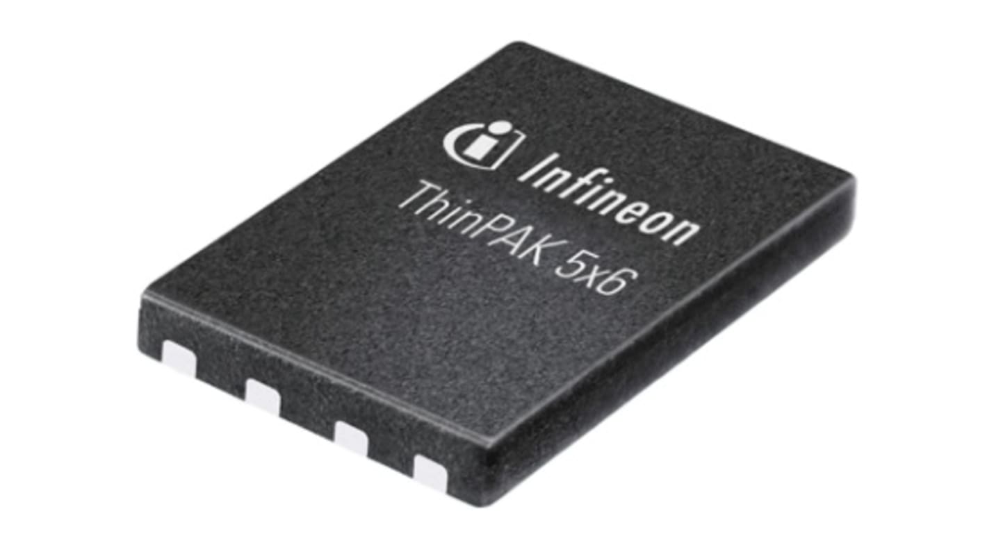
รูปภาพประกอบสินค้าเป็นเพียงรูปภาพใกล้เคียงเท่านั้น กรุณาอ่านรายละเอียดสินค้า
มีส่วนลดเมื่อซื้อจำนวนมาก
ดูตัวเลือกการกำหนดราคาในการซื้อปริมาณมากยอดรวมย่อย (1 แพ็ค แพ็คละ 10 ชิ้น)*
THB487.70
(ไม่รวมภาษีมูลค่าเพิ่ม)
THB521.80
(รวมภาษีมูลค่าเพิ่ม)
ส่งฟรีหากซื้อเกิน ฿2,500.00
สต็อกสุดท้ายของ RS
- 5,470 ชิ้นสุดท้ายพร้อมจัดส่งจากคลังสินค้าต่างประเทศ
ชิ้น | ต่อหน่วย | ต่อแพ็ค* |
|---|---|---|
| 10 - 1240 | THB48.77 | THB487.70 |
| 1250 - 2490 | THB47.551 | THB475.51 |
| 2500 + | THB46.821 | THB468.21 |
*ตัวบ่งบอกราคา / price indicative
- RS Stock No.:
- 220-7435
- หมายเลขชิ้นส่วนของผู้ผลิต / Mfr. Part No.:
- IPL60R360P6SATMA1
- ผู้ผลิต:
- Infineon
คุณสมบัติ / Specifications
ข้อมูลทางเทคนิค / Technical Data Sheets
Legislation and Compliance
รายละเอียดสินค้า / Product Details
ค้นหาผลิตภัณฑ์ที่คล้ายกันโดยเลือกคุณลักษณะอย่างน้อยหนึ่งรายการ
เลือกทั้งหมด | คุณลักษณะ | ค่า |
|---|---|---|
| Brand | Infineon | |
| Product Type | MOSFET & Diode | |
| Channel Type | Type N | |
| Maximum Continuous Drain Current Id | 30A | |
| Maximum Drain Source Voltage Vds | 650V | |
| Package Type | ThinPAK | |
| Series | CoolMOS P6 | |
| Mount Type | Surface | |
| Pin Count | 5 | |
| Maximum Drain Source Resistance Rds | 360mΩ | |
| Channel Mode | Enhancement | |
| Maximum Power Dissipation Pd | 89.3W | |
| Typical Gate Charge Qg @ Vgs | 22nC | |
| Minimum Operating Temperature | -40°C | |
| Forward Voltage Vf | 0.9V | |
| Maximum Operating Temperature | 150°C | |
| Height | 1.1mm | |
| Length | 5.1mm | |
| Standards/Approvals | No | |
| Automotive Standard | No | |
| เลือกทั้งหมด | ||
|---|---|---|
Brand Infineon | ||
Product Type MOSFET & Diode | ||
Channel Type Type N | ||
Maximum Continuous Drain Current Id 30A | ||
Maximum Drain Source Voltage Vds 650V | ||
Package Type ThinPAK | ||
Series CoolMOS P6 | ||
Mount Type Surface | ||
Pin Count 5 | ||
Maximum Drain Source Resistance Rds 360mΩ | ||
Channel Mode Enhancement | ||
Maximum Power Dissipation Pd 89.3W | ||
Typical Gate Charge Qg @ Vgs 22nC | ||
Minimum Operating Temperature -40°C | ||
Forward Voltage Vf 0.9V | ||
Maximum Operating Temperature 150°C | ||
Height 1.1mm | ||
Length 5.1mm | ||
Standards/Approvals No | ||
Automotive Standard No | ||
The Infineon new Cool MOS Thin PAK 5x6 is a leadless SMD package especially designed for high voltage MOSFETs. This new package has a very small footprint of 5x6mm 2 and a very low profile with only 1mm height. This significantly smaller package size in combination with its benchmark low parasitic inductances can be used as a new and effective way to decrease system solution size in power- density driven designs. The Thin PAK 5x6 package is characterized by a very low source inductance 1.6nH, as well as a similar thermal performance as DPAK. The package hence enables faster and thus more efficient switching of power MOSFETs and is easier to handle in terms of switching behaviour and EMI.
Extremely low losses due to very low FOMRdson*Qg and Eoss
Very high commutation ruggedness
Easy to use/drive
Pb-freeplating, Halogen free mold compound
Qualified for industrial grade applications according to JEDEC
ลิงก์ที่เกี่ยวข้อง
- Infineon CoolMOS P6 Type N-Channel MOSFET & Diode 650 V Enhancement, 5-Pin ThinPAK
- Infineon 600V CoolMOS CFD7 Type N-Channel MOSFET 650 V Enhancement, 5-Pin ThinPAK
- Infineon CoolMOS P6 Type N-Channel MOSFET 600 V Enhancement, 5-Pin VSON
- Infineon CoolMOS P6 Type N-Channel MOSFET 600 V Enhancement, 5-Pin VSON
- Infineon CoolMOS P6 Type N-Channel MOSFET 600 V Enhancement, 5-Pin VSON IPL60R180P6AUMA1
- Infineon CoolMOS P6 Type N-Channel MOSFET 600 V Enhancement, 5-Pin VSON IPL60R210P6AUMA1
- Infineon 600V CoolMOS CFD7 Type N-Channel MOSFET 650 V Enhancement, 5-Pin ThinPAK IPL60R185CFD7AUMA1
- Infineon CoolMOS P6 Type N-Channel MOSFET & Diode 650 V Enhancement, 3-Pin TO-247