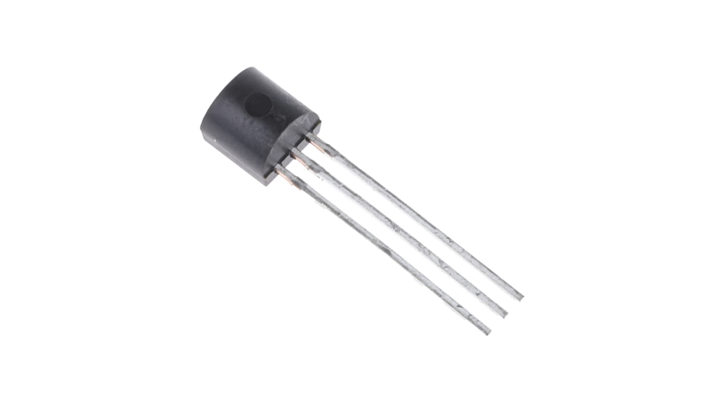
Microchip 2N7000 Type N-Channel MOSFET, 200 mA, 60 V Enhancement, 3-Pin TO-92 2N7000-G
- RS Stock No.:
- 177-9760
- Distrelec หมายเลขบทความ:
- 304-38-475
- หมายเลขชิ้นส่วนของผู้ผลิต / Mfr. Part No.:
- 2N7000-G
- ผู้ผลิต:
- Microchip

รูปภาพประกอบสินค้าเป็นเพียงรูปภาพใกล้เคียงเท่านั้น กรุณาอ่านรายละเอียดสินค้า
ยอดรวมย่อย (1 แพ็ค แพ็คละ 25 ชิ้น)*
THB359.575
(ไม่รวมภาษีมูลค่าเพิ่ม)
THB384.75
(รวมภาษีมูลค่าเพิ่ม)
ส่งฟรีหากซื้อเกิน ฿2,500.00
มีในสต็อก
- เพิ่มอีก 500 ชิ้นจะส่งได้หลังจากวันที่ 13 กรกฎาคม 2569 ไปอีกประมาณ 7 วันทำการ
- เพิ่มอีก 2,600 ชิ้นจะส่งได้หลังจากวันที่ 20 กรกฎาคม 2569 ไปอีกประมาณ 7 วันทำการ
ต้องการสินค้าเพิ่มหรือไม่ ระบุจำนวนและคลิก ‘ตรวจสอบวันจัดส่ง’ เพื่อดูข้อมูลเพิ่มเติมเกี่ยวกับสต็อกสินค้าและการจัดส่ง
ชิ้น | ต่อหน่วย | ต่อแพ็ค* |
|---|---|---|
| 25 + | THB14.383 | THB359.58 |
*ตัวบ่งบอกราคา / price indicative
- RS Stock No.:
- 177-9760
- Distrelec หมายเลขบทความ:
- 304-38-475
- หมายเลขชิ้นส่วนของผู้ผลิต / Mfr. Part No.:
- 2N7000-G
- ผู้ผลิต:
- Microchip
คุณสมบัติ / Specifications
ข้อมูลทางเทคนิค / Technical Data Sheets
Legislation and Compliance
รายละเอียดสินค้า / Product Details
ค้นหาผลิตภัณฑ์ที่คล้ายกันโดยเลือกคุณลักษณะอย่างน้อยหนึ่งรายการ
เลือกทั้งหมด | คุณลักษณะ | ค่า |
|---|---|---|
| Brand | Microchip | |
| Channel Type | Type N | |
| Product Type | MOSFET | |
| Maximum Continuous Drain Current Id | 200mA | |
| Maximum Drain Source Voltage Vds | 60V | |
| Series | 2N7000 | |
| Package Type | TO-92 | |
| Mount Type | Through Hole | |
| Pin Count | 3 | |
| Maximum Drain Source Resistance Rds | 5.3Ω | |
| Channel Mode | Enhancement | |
| Maximum Power Dissipation Pd | 1W | |
| Minimum Operating Temperature | -55°C | |
| Forward Voltage Vf | 0.85V | |
| Maximum Operating Temperature | 150°C | |
| Standards/Approvals | No | |
| Height | 5.33mm | |
| Length | 5.08mm | |
| Automotive Standard | No | |
| เลือกทั้งหมด | ||
|---|---|---|
Brand Microchip | ||
Channel Type Type N | ||
Product Type MOSFET | ||
Maximum Continuous Drain Current Id 200mA | ||
Maximum Drain Source Voltage Vds 60V | ||
Series 2N7000 | ||
Package Type TO-92 | ||
Mount Type Through Hole | ||
Pin Count 3 | ||
Maximum Drain Source Resistance Rds 5.3Ω | ||
Channel Mode Enhancement | ||
Maximum Power Dissipation Pd 1W | ||
Minimum Operating Temperature -55°C | ||
Forward Voltage Vf 0.85V | ||
Maximum Operating Temperature 150°C | ||
Standards/Approvals No | ||
Height 5.33mm | ||
Length 5.08mm | ||
Automotive Standard No | ||
- COO (Country of Origin):
- TW
Microchip Technology MOSFET
The Microchip Technology through-hole mount N-channel MOSFET is a new age product with a drain-source voltage of 60V and a maximum gate-source voltage of 30V. It has drain-source resistance of 5ohms at a gate-source voltage of 10V. It has continuous drain current of 200mA and maximum power dissipation of 1W. The minimum and a maximum driving voltage for this MOSFET is 4.5V and 10V respectively. The MOSFET is an enhancement mode (normally off) MOSFET that utilizes a vertical DMOS structure and well-proven, silicon gate manufacturing process. This combination produces a device with the power handling capabilities of bipolar transistors and the high input impedance and positive temperature coefficient inherent in MOS devices. A significant characteristic of all MOS structures, this device is free from thermal runaway and thermally induced secondary breakdown. This vertical DMOS FET has been optimized for lower switching and conduction losses. The MOSFET offers excellent efficiency along with a long and productive life without compromising performance or functionality.
Features and Benefits
• Ease of paralleling
• Excellent thermal stability
• Free from secondary breakdown
• High input impedance and high gain
• Integral source drain diode
• Low CISS and fast switching speeds
• Low power drive requirement
• Operating temperature ranges between -55°C and 150°C
Applications
• Amplifiers
• Converters
• Drivers: relays, hammers, solenoids, lamps, memories, displays, bipolar transistors, etc.
• Motor controls
• Power supply circuits
• Switches
Certifications
• ANSI/ESD S20.20:2014
• BS EN 61340-5-1:2007
• JEDEC
ลิงก์ที่เกี่ยวข้อง
- Microchip 2N7000 Type N-Channel MOSFET 60 V Enhancement, 3-Pin TO-92
- onsemi 2N7000 Type N-Channel MOSFET 60 V Enhancement, 3-Pin TO-92 2N7000-D26Z
- onsemi 2N7000 Type N-Channel MOSFET 60 V Enhancement, 3-Pin TO-92
- onsemi 2N7000 Type N-Channel MOSFET 60 V Enhancement, 3-Pin TO-92 2N7000
- onsemi 2N7000 Type N-Channel MOSFET 60 V Enhancement, 3-Pin TO-92 2N7000TA
- DiodesZetex Type N-Channel MOSFET 60 V Enhancement, 3-Pin SOT-23
- Infineon SIPMOS Type N-Channel MOSFET 60 V Enhancement, 3-Pin SOT-23 SN7002NH6327XTSA2
- Infineon SN7002I Type N-Channel MOSFET 60 V Enhancement, 3-Pin SOT-23 SN7002IXTSA1