Toshiba 74VHC126FT Non-Inverting 3 State Octal Bus Buffer, 14-Pin TSSOP
- RS Stock No.:
- 171-3395
- หมายเลขชิ้นส่วนของผู้ผลิต / Mfr. Part No.:
- 74VHC126FT
- ผู้ผลิต:
- Toshiba

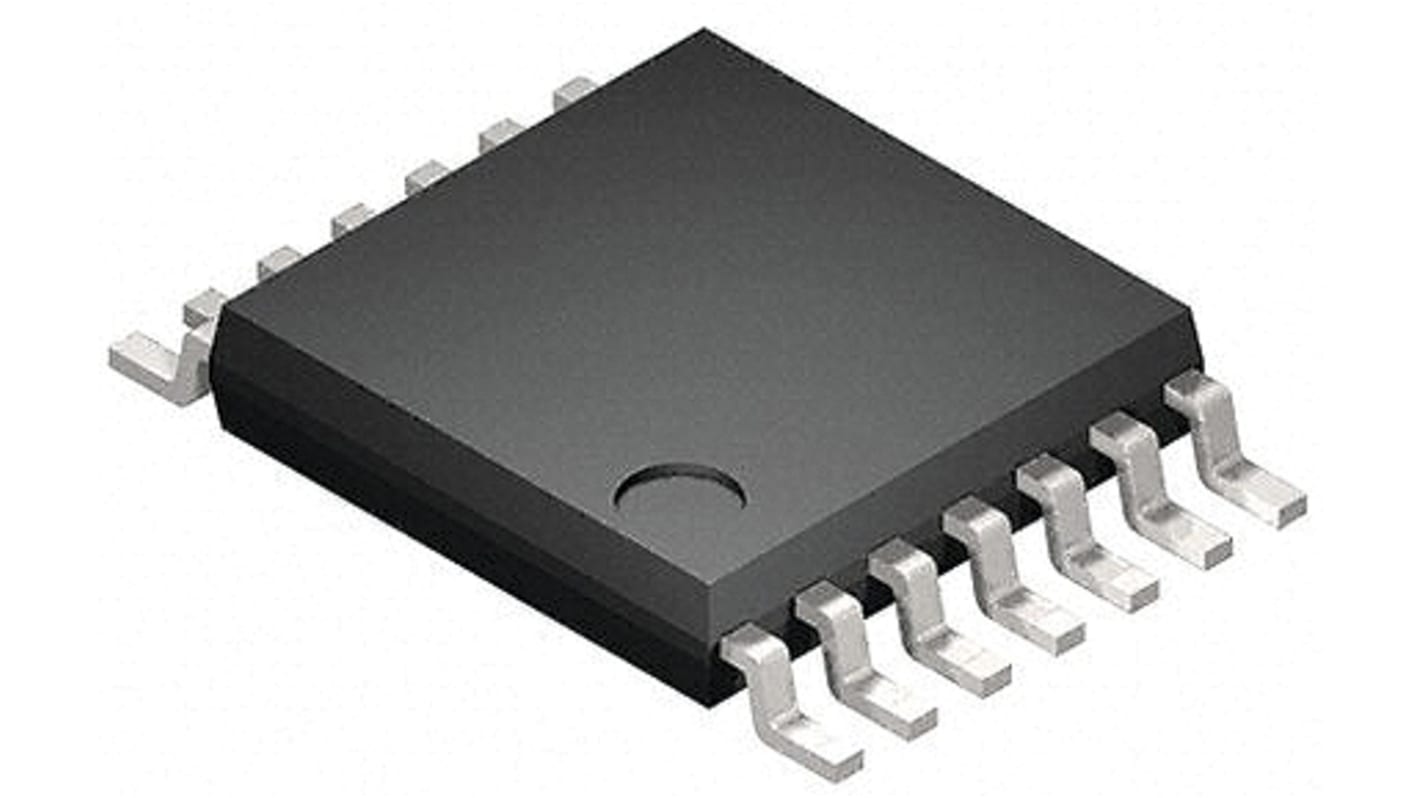
รูปภาพประกอบสินค้าเป็นเพียงรูปภาพใกล้เคียงเท่านั้น กรุณาอ่านรายละเอียดสินค้า
มีส่วนลดเมื่อซื้อจำนวนมาก
ดูตัวเลือกการกำหนดราคาในการซื้อปริมาณมากยอดรวมย่อย (1 แพ็ค แพ็คละ 50 ชิ้น)*
THB703.85
(ไม่รวมภาษีมูลค่าเพิ่ม)
THB753.10
(รวมภาษีมูลค่าเพิ่ม)
ส่งฟรีหากซื้อเกิน ฿2,500.00
สต็อกสุดท้ายของ RS
- 750 ชิ้นสุดท้ายพร้อมจัดส่งจากคลังสินค้าต่างประเทศ
ชิ้น | ต่อหน่วย | ต่อแพ็ค* |
|---|---|---|
| 50 - 600 | THB14.077 | THB703.85 |
| 650 - 1200 | THB13.726 | THB686.30 |
| 1250 + | THB13.514 | THB675.70 |
*ตัวบ่งบอกราคา / price indicative
- RS Stock No.:
- 171-3395
- หมายเลขชิ้นส่วนของผู้ผลิต / Mfr. Part No.:
- 74VHC126FT
- ผู้ผลิต:
- Toshiba
คุณสมบัติ / Specifications
ข้อมูลทางเทคนิค / Technical Data Sheets
Legislation and Compliance
รายละเอียดสินค้า / Product Details
ค้นหาผลิตภัณฑ์ที่คล้ายกันโดยเลือกคุณลักษณะอย่างน้อยหนึ่งรายการ
เลือกทั้งหมด | คุณลักษณะ | ค่า |
|---|---|---|
| Brand | Toshiba | |
| Logic Family | 74VHC | |
| Product Type | Octal Bus Buffer | |
| Logic Function | Buffer | |
| Schmitt Trigger Input | No | |
| Input Type | CMOS | |
| Mount Type | Surface | |
| Output Type | 3 State | |
| Polarity | Non-Inverting | |
| Minimum Supply Voltage | 2V | |
| Package Type | TSSOP | |
| Pin Count | 14 | |
| Maximum Supply Voltage | 5.5V | |
| Maximum High Level Output Current | -8mA | |
| Minimum Operating Temperature | -40°C | |
| Maximum Propagation Delay Time @ CL | 3.8ns | |
| Maximum Low Level Output Current | 8mA | |
| Maximum Operating Temperature | 125°C | |
| Series | 74VHC | |
| Standards/Approvals | No | |
| Height | 1mm | |
| Length | 5mm | |
| Automotive Standard | AEC-Q100 | |
| Supply Current | 4μA | |
| เลือกทั้งหมด | ||
|---|---|---|
Brand Toshiba | ||
Logic Family 74VHC | ||
Product Type Octal Bus Buffer | ||
Logic Function Buffer | ||
Schmitt Trigger Input No | ||
Input Type CMOS | ||
Mount Type Surface | ||
Output Type 3 State | ||
Polarity Non-Inverting | ||
Minimum Supply Voltage 2V | ||
Package Type TSSOP | ||
Pin Count 14 | ||
Maximum Supply Voltage 5.5V | ||
Maximum High Level Output Current -8mA | ||
Minimum Operating Temperature -40°C | ||
Maximum Propagation Delay Time @ CL 3.8ns | ||
Maximum Low Level Output Current 8mA | ||
Maximum Operating Temperature 125°C | ||
Series 74VHC | ||
Standards/Approvals No | ||
Height 1mm | ||
Length 5mm | ||
Automotive Standard AEC-Q100 | ||
Supply Current 4μA | ||
The 74VHC125FT,74VHC126FT are high speed CMOS QUAD BUS BUFFERs fabricated with silicon gate C2MOS technology. They achieve the high speed operation similar to equivalent Bipolar Shottky TTL while maintaining the CMOS low power dissipation. The 74VHC125FT requires the 3-state control input G to be set high to place the output into the high impedance state, whereas the 74VHC126FT requires the control input G to be set low to place the output into high impedance. An input protection circuit ensures that 0 to 5.5 V can be applied to the input pins without regard to the supply voltage. This device can be used to interface 5 V to 3 V systems and two supply systems such as battery back up This circuit prevents device destruction due to mismatched supply and input voltages
Wide operating temperature: Topr = -40 to 125
High speed: Propagation delay time = 3.8 ns (typ.) at VCC = 5.0 V
Low power dissipation: ICC = 2.0 μA (max) at Ta = 25
High noise immunity: VNIH = VNIL = 28 % VCC (min)
Power-down protection is provided on all inputs.
Balanced propagation delays: tPLH ≈ tPHL
Wide operating voltage range: VCC(opr) = 2.0 to 5.5 V
Low noise: V = 0.8 V (max)
ลิงก์ที่เกี่ยวข้อง
- Toshiba 74VHCT126AFT Non-Inverting 3 State Octal Bus Buffer, 14-Pin TSSOP
- Toshiba 74HC244D Non-Inverting 3 State Octal Bus Buffer, 20-Pin SOIC
- Toshiba Non-Inverting 3 State Octal Bus Buffer, 20-Pin SOIC
- Toshiba 74HC126D Schmitt Trigger Input 3 State Octal Bus Buffer, 14-Pin SOIC
- Toshiba 74VHCT125AFT Non-Inverting 3 State Quad Bus Buffer, 14-Pin TSSOP
- Toshiba 3 State Octal Bus Buffer, 20-Pin TSSOP
- Toshiba 74VHCT541AFT 3 State Octal Bus Buffer, 20-Pin TSSOP
- Toshiba 74VHC540FT 3 State Octal Bus Buffer, 20-Pin TSSOP