Toshiba 74VHC221AFT, 27 Dual Monostable Multivibrator 74VHC 8 mA, 16-Pin TSSOP
- RS Stock No.:
- 171-3459
- หมายเลขชิ้นส่วนของผู้ผลิต / Mfr. Part No.:
- 74VHC221AFT
- ผู้ผลิต:
- Toshiba

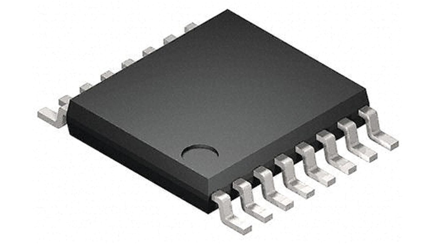
รูปภาพประกอบสินค้าเป็นเพียงรูปภาพใกล้เคียงเท่านั้น กรุณาอ่านรายละเอียดสินค้า
ยอดรวมย่อย (1 แพ็ค แพ็คละ 50 ชิ้น)*
THB305.40
(ไม่รวมภาษีมูลค่าเพิ่ม)
THB326.80
(รวมภาษีมูลค่าเพิ่ม)
ส่งฟรีหากซื้อเกิน ฿2,500.00
- 200 ชิ้นจะส่งได้หลังจากวันที่ 29 มิถุนายน 2569 ไปอีกประมาณ 7 วันทำการ
ชิ้น | ต่อหน่วย | ต่อแพ็ค* |
|---|---|---|
| 50 - 600 | THB6.108 | THB305.40 |
| 650 - 1200 | THB5.955 | THB297.75 |
| 1250 + | THB5.864 | THB293.20 |
*ตัวบ่งบอกราคา / price indicative
- RS Stock No.:
- 171-3459
- หมายเลขชิ้นส่วนของผู้ผลิต / Mfr. Part No.:
- 74VHC221AFT
- ผู้ผลิต:
- Toshiba
เลือกทั้งหมด | คุณลักษณะ | ค่า |
|---|---|---|
| Brand | Toshiba | |
| Logic Family | 74VHC | |
| Product Type | Dual Monostable Multivibrator | |
| Number of Elements per Chip | 27 | |
| Maximum High Level Output Current | -8mA | |
| Maximum Low Level Output Current | 8mA | |
| Minimum Pulse Width | 5ns | |
| Maximum Quiescent Current | 80μA | |
| Minimum Supply Voltage | 2V | |
| Mount Type | Surface | |
| Package Type | TSSOP | |
| Maximum Supply Voltage | 5.5V | |
| Pin Count | 16 | |
| Multivibrator Type | Monostable Multivibrator | |
| Minimum Operating Temperature | -40°C | |
| Maximum Propagation Delay Time @ CL | 8.1ns | |
| Maximum Operating Temperature | 125°C | |
| Height | 1mm | |
| Standards/Approvals | No | |
| Series | 74VHC221AFT | |
| Length | 5mm | |
| Automotive Standard | AEC-Q100 | |
| เลือกทั้งหมด | ||
|---|---|---|
Brand Toshiba | ||
Logic Family 74VHC | ||
Product Type Dual Monostable Multivibrator | ||
Number of Elements per Chip 27 | ||
Maximum High Level Output Current -8mA | ||
Maximum Low Level Output Current 8mA | ||
Minimum Pulse Width 5ns | ||
Maximum Quiescent Current 80μA | ||
Minimum Supply Voltage 2V | ||
Mount Type Surface | ||
Package Type TSSOP | ||
Maximum Supply Voltage 5.5V | ||
Pin Count 16 | ||
Multivibrator Type Monostable Multivibrator | ||
Minimum Operating Temperature -40°C | ||
Maximum Propagation Delay Time @ CL 8.1ns | ||
Maximum Operating Temperature 125°C | ||
Height 1mm | ||
Standards/Approvals No | ||
Series 74VHC221AFT | ||
Length 5mm | ||
Automotive Standard AEC-Q100 | ||
ลิงก์ที่เกี่ยวข้อง
- Toshiba 16-Pin TSSOP
- Toshiba 74VHC123AFT 16-Pin TSSOP
- Nexperia 16-Pin TSSOP
- Nexperia 16-Pin TSSOP
- Nexperia 74HC4538PW 2 Dual Monostable Multivibrator HC 5.2 mA, 16-Pin TSSOP
- Nexperia 16-Pin TSSOP
- Nexperia 74HC123PW 2 Dual Monostable Multivibrator HC 4 mA, 16-Pin TSSOP
- Nexperia 74HC123PW-Q100 2 Dual Monostable Multivibrator 74HC 5.2 mA, 16-Pin TSSOP