Toshiba 74HC4050D 6-Channel Buffer & Line Driver, CMOS, Non-Inverting, 16-Pin SOIC
- RS Stock No.:
- 171-3601
- หมายเลขชิ้นส่วนของผู้ผลิต / Mfr. Part No.:
- 74HC4050D
- ผู้ผลิต:
- Toshiba

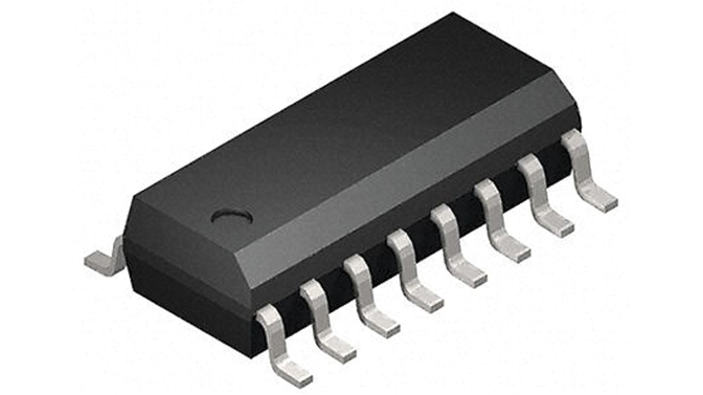
รูปภาพประกอบสินค้าเป็นเพียงรูปภาพใกล้เคียงเท่านั้น กรุณาอ่านรายละเอียดสินค้า
ยอดรวมย่อย (1 แพ็ค แพ็คละ 20 ชิ้น)*
THB225.66
(ไม่รวมภาษีมูลค่าเพิ่ม)
THB241.46
(รวมภาษีมูลค่าเพิ่ม)
ส่งฟรีหากซื้อเกิน ฿2,500.00
มีในสต็อก
- 180 ชิ้นพร้อมจัดส่งจากคลังสินค้าต่างประเทศ
- เพิ่มอีก 740 ชิ้นจะส่งได้หลังจากวันที่ 23 กรกฎาคม 2569 ไปอีกประมาณ 7 วันทำการ
ต้องการสินค้าเพิ่มหรือไม่ ระบุจำนวนและคลิก ‘ตรวจสอบวันจัดส่ง’ เพื่อดูข้อมูลเพิ่มเติมเกี่ยวกับสต็อกสินค้าและการจัดส่ง
ชิ้น | ต่อหน่วย | ต่อแพ็ค* |
|---|---|---|
| 20 + | THB11.283 | THB225.66 |
*ตัวบ่งบอกราคา / price indicative
- RS Stock No.:
- 171-3601
- หมายเลขชิ้นส่วนของผู้ผลิต / Mfr. Part No.:
- 74HC4050D
- ผู้ผลิต:
- Toshiba
คุณสมบัติ / Specifications
ข้อมูลทางเทคนิค / Technical Data Sheets
Legislation and Compliance
รายละเอียดสินค้า / Product Details
ค้นหาผลิตภัณฑ์ที่คล้ายกันโดยเลือกคุณลักษณะอย่างน้อยหนึ่งรายการ
เลือกทั้งหมด | คุณลักษณะ | ค่า |
|---|---|---|
| Brand | Toshiba | |
| Product Type | Buffer & Line Driver | |
| Logic Family | 74HC | |
| Logic Function | Buffer & Line Driver | |
| IC Type | Hex Buffer | |
| Number of Channels | 6 | |
| Output Type | CMOS | |
| Polarity | Non-Inverting | |
| Mount Type | Surface | |
| Package Type | SOIC | |
| Pin Count | 16 | |
| Minimum Supply Voltage | 2V | |
| Maximum Supply Voltage | 6V | |
| Maximum High Level Output Current | -7.8mA | |
| Minimum Operating Temperature | -40°C | |
| Maximum Low Level Output Current | 7.8mA | |
| Maximum Propagation Delay Time @ CL | 100ns | |
| Maximum Operating Temperature | 85°C | |
| Length | 10.2mm | |
| Series | 74HC | |
| Standards/Approvals | No | |
| Height | 1.75mm | |
| Automotive Standard | No | |
| Supply Current | 10μA | |
| เลือกทั้งหมด | ||
|---|---|---|
Brand Toshiba | ||
Product Type Buffer & Line Driver | ||
Logic Family 74HC | ||
Logic Function Buffer & Line Driver | ||
IC Type Hex Buffer | ||
Number of Channels 6 | ||
Output Type CMOS | ||
Polarity Non-Inverting | ||
Mount Type Surface | ||
Package Type SOIC | ||
Pin Count 16 | ||
Minimum Supply Voltage 2V | ||
Maximum Supply Voltage 6V | ||
Maximum High Level Output Current -7.8mA | ||
Minimum Operating Temperature -40°C | ||
Maximum Low Level Output Current 7.8mA | ||
Maximum Propagation Delay Time @ CL 100ns | ||
Maximum Operating Temperature 85°C | ||
Length 10.2mm | ||
Series 74HC | ||
Standards/Approvals No | ||
Height 1.75mm | ||
Automotive Standard No | ||
Supply Current 10μA | ||
The 74HC4049D and 74HC4050D are high speed CMOS HEX BUFFERs fabricated with silicon gate C2MOS technology. They achieve the high speed operation similar to equivalent LSTTL while maintaining the CMOS low power dissipation. The 74HC4049D is an inverting buffer, while the 74HC4050D is a non-inverting buffer. The internal circuits are composed of 3-stages (74HC4049D) or 2-stages (74HC4050D) of inverter, which provided high noise immunity and stable output. Input protection circuits are different from those of other high speed CMOS IC's. They eliminate the diodes on the VCC side thus providing of logic-level conversion from high-level voltages up to 15 V to low-level voltages. They are useful for battery back up circuits, because input voltage can be applied on IC's which are not biased by VCC
High speed: tpd = 8 ns (typ.) at VCC = 6.0 V
Low power dissipation: ICC = 1.0 μA (max) at Ta = 25
Balanced propagation delays: tPLH ≈ tPHL
Wide operating voltage range: VCC(opr) = 2.0 V to 6.0 V
ลิงก์ที่เกี่ยวข้อง
- Toshiba 6-Channel Buffer & Line Driver Non-Inverting, 16-Pin SOIC
- Toshiba TC7SH17FU CMOS 5-Pin SSOP
- Toshiba TC74HC4050AP(F) 6-Channel Buffer & Line Driver Non-Inverting, 16-Pin PDIP
- Toshiba TC4050BF(N 3 State 16-Pin SOP
- Toshiba TC4050BP(N 3 State 16-Pin PDIP
- onsemi MC74HC245ADWG Buffer & Line Driver Non-Inverting, 20-Pin SOIC
- Texas Instruments CD74HCT365M 6-Channel Buffer & Line Driver Non-Inverting, 16-Pin SOIC
- onsemi MC74HC245ADTG Buffer & Line Driver Non-Inverting, 20-Pin TSSOP