Infineon NOR 256 MB SPI Flash Memory 24-Pin BGA, S25FL256LAGBHV020
- RS Stock No.:
- 184-0071
- หมายเลขชิ้นส่วนของผู้ผลิต / Mfr. Part No.:
- S25FL256LAGBHV020
- ผู้ผลิต:
- Infineon

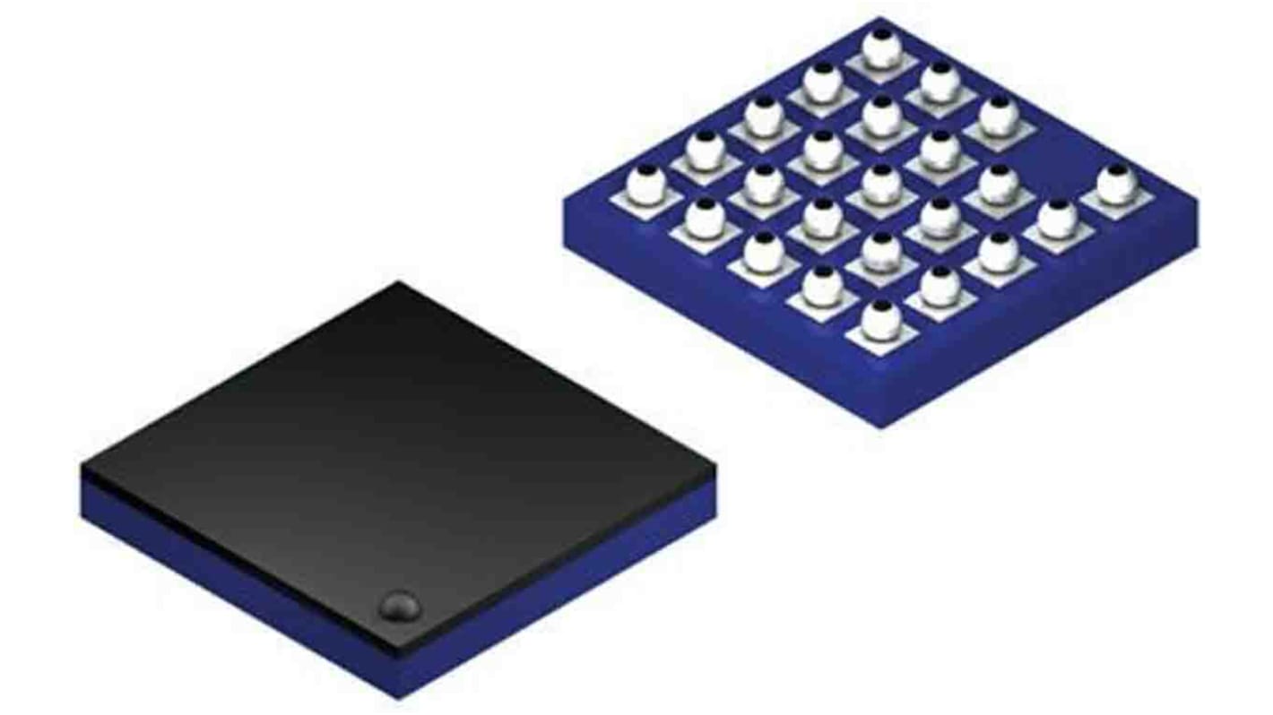
รูปภาพประกอบสินค้าเป็นเพียงรูปภาพใกล้เคียงเท่านั้น กรุณาอ่านรายละเอียดสินค้า
มีส่วนลดเมื่อซื้อจำนวนมาก
ดูตัวเลือกการกำหนดราคาในการซื้อปริมาณมากยอดรวมย่อย (1 แพ็ค แพ็คละ 2 ชิ้น)*
THB276.58
(ไม่รวมภาษีมูลค่าเพิ่ม)
THB295.94
(รวมภาษีมูลค่าเพิ่ม)
ส่งฟรีหากซื้อเกิน ฿2,500.00
มีในสต็อก
- 1,346 ชิ้นพร้อมจัดส่งจากคลังสินค้าต่างประเทศ
ต้องการสินค้าเพิ่มหรือไม่ ระบุจำนวนและคลิก ‘ตรวจสอบวันจัดส่ง’ เพื่อดูข้อมูลเพิ่มเติมเกี่ยวกับสต็อกสินค้าและการจัดส่ง
ชิ้น | ต่อหน่วย | ต่อแพ็ค* |
|---|---|---|
| 2 - 84 | THB138.29 | THB276.58 |
| 86 - 168 | THB134.83 | THB269.66 |
| 170 + | THB132.75 | THB265.50 |
*ตัวบ่งบอกราคา / price indicative
- RS Stock No.:
- 184-0071
- หมายเลขชิ้นส่วนของผู้ผลิต / Mfr. Part No.:
- S25FL256LAGBHV020
- ผู้ผลิต:
- Infineon
คุณสมบัติ / Specifications
ข้อมูลทางเทคนิค / Technical Data Sheets
Legislation and Compliance
รายละเอียดสินค้า / Product Details
ค้นหาผลิตภัณฑ์ที่คล้ายกันโดยเลือกคุณลักษณะอย่างน้อยหนึ่งรายการ
เลือกทั้งหมด | คุณลักษณะ | ค่า |
|---|---|---|
| Brand | Infineon | |
| Product Type | Flash Memory | |
| Memory Size | 256MB | |
| Interface Type | SPI | |
| Package Type | BGA | |
| Pin Count | 24 | |
| Organisation | 32M x 8 bit | |
| Mount Type | Surface | |
| Maximum Clock Frequency | 133MHz | |
| Cell Type | NOR | |
| Maximum Supply Voltage | 3.6V | |
| Minimum Supply Voltage | 2.7V | |
| Timing Type | Synchronous | |
| Minimum Operating Temperature | -40°C | |
| Maximum Operating Temperature | 105°C | |
| Standards/Approvals | No | |
| Width | 6mm | |
| Length | 6mm | |
| Height | 0.95mm | |
| Number of Bits per Word | 8 | |
| Series | S25FL256L | |
| Maximum Random Access Time | 8ns | |
| Automotive Standard | AEC-Q100 | |
| Number of Words | 32M | |
| เลือกทั้งหมด | ||
|---|---|---|
Brand Infineon | ||
Product Type Flash Memory | ||
Memory Size 256MB | ||
Interface Type SPI | ||
Package Type BGA | ||
Pin Count 24 | ||
Organisation 32M x 8 bit | ||
Mount Type Surface | ||
Maximum Clock Frequency 133MHz | ||
Cell Type NOR | ||
Maximum Supply Voltage 3.6V | ||
Minimum Supply Voltage 2.7V | ||
Timing Type Synchronous | ||
Minimum Operating Temperature -40°C | ||
Maximum Operating Temperature 105°C | ||
Standards/Approvals No | ||
Width 6mm | ||
Length 6mm | ||
Height 0.95mm | ||
Number of Bits per Word 8 | ||
Series S25FL256L | ||
Maximum Random Access Time 8ns | ||
Automotive Standard AEC-Q100 | ||
Number of Words 32M | ||
- COO (Country of Origin):
- US
Serial Peripheral Interface (SPI) with Multi-I/O
Clock polarity and phase modes 0 and 3
Double Data Rate (DDR) option
Quad peripheral Interface (QPI) option
Extended Addressing: 24- or 32-bit address options
Serial Command subset and footprint compatible with S25FL-A, S25FL1-K, S25FL-P, S25FL-S and S25FS-S SPI families
Multi I/O Command subset and footprint compatible with S25FL-P, S25FL-S and S25FS-S SPI families
Read
Commands: Normal, Fast, Dual I/O, Quad I/O, DualO,QuadO, DDR Quad I/O.
Modes: Burst Wrap, Continuous (XIP), QPI
Serial Flash Discoverable Parameters (SFDP) for configuration information.
Program Architecture
256 Bytes Page Programming buffer
3.0 V FL-L Flash Memory
Program suspend and resume
Erase Architecture
Uniform 4 KB Sector Erase
Uniform 32 KB Half Block Erase
Uniform 64 KB Block Erase
Chip erase
Erase suspend and resume
100,000 Program/Erase Cycles, minimum
20 Year Data Retention, minimum
Security features
Status and Configuration Register Protection
Four Security Regions of 256 bytes each outside the main
Flash array
Legacy Block Protection: Block range
Individual and Region Protection
Individual Block Lock: Volatile individual Sector/Block
Pointer Region: Non-Volatile Sector/Block range
Power Supply Lock-down, Password, or Permanent protection of Security Regions 2 and 3 and Pointer Region
Technology
65 nm Floating Gate Technology
Single Supply Voltage with CMOS I/O
2.7 V to 3.6 V
Packages (all Pb-free)
8-pin SOIC 208 mil (SOC008) — S25FL128L only
WSON 5 x 6 mm (WND008) — S25FL128L only
WSON 6 x 8 mm (WNG008) — S25FL256L only
16-pin SOIC 300 mil (SO3016)
BGA-24 6 x 8 mm
5 x 5 ball (FAB024) footprint
4 x 6 ball (FAC024) footprint
ลิงก์ที่เกี่ยวข้อง
- Infineon NOR 256 MB SPI Flash Memory 24-Pin BGA
- Infineon NOR 256 MB SPI Flash Memory 24-Pin BGA, S25FL256SAGBHV200
- Infineon NOR 512 MB SPI Flash Memory 24-Pin BGA, S25HS512TDPBHI010
- Infineon NOR 512 MB SPI Flash Memory 24-Pin BGA, S26HS512TGABHI010
- Infineon NOR 512 MB SPI Flash Memory 24-Pin BGA
- Infineon NOR 512 MB SPI Flash Memory 24-Pin BGA, S25HL512TFABHI010
- Infineon NOR 512 MB SPI Flash Memory 24-Pin BGA, S26HL512TFPBHI000
- Infineon NOR 512 MB SPI Flash Memory 24-Pin BGA, S25HS512TFABHI010