Toshiba, Decoder, 16-Pin TSSOP
- RS Stock No.:
- 171-3433P
- หมายเลขชิ้นส่วนของผู้ผลิต / Mfr. Part No.:
- 74VHC138FT
- ผู้ผลิต:
- Toshiba

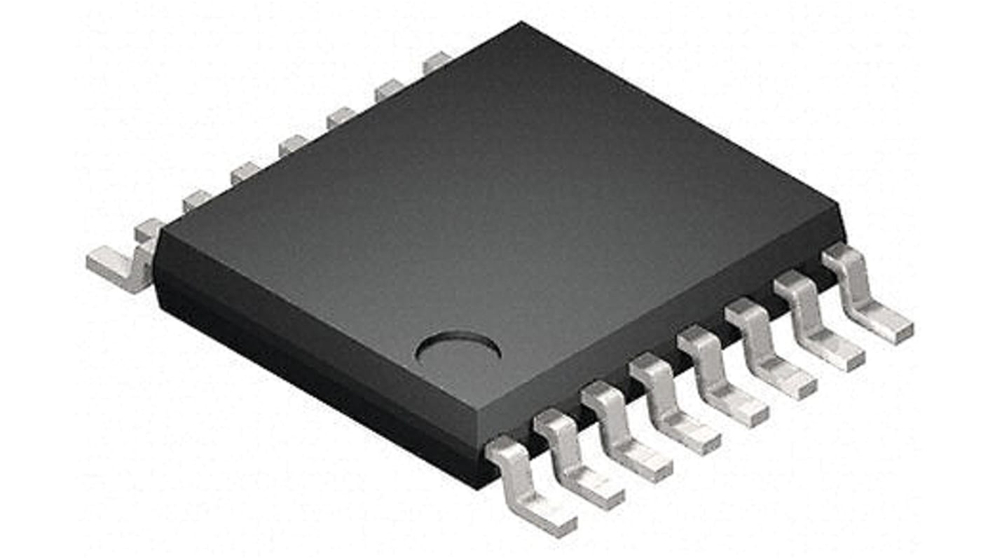
รูปภาพประกอบสินค้าเป็นเพียงรูปภาพใกล้เคียงเท่านั้น กรุณาอ่านรายละเอียดสินค้า
มีส่วนลดเมื่อซื้อจำนวนมาก
ดูตัวเลือกการกำหนดราคาในการซื้อปริมาณมากยอดรวมย่อย 650 ชิ้น (จัดส่งเป็นม้วน)*
THB10,091.90
(ไม่รวมภาษีมูลค่าเพิ่ม)
THB10,798.45
(รวมภาษีมูลค่าเพิ่ม)
ส่งฟรีหากซื้อเกิน ฿2,500.00
หมดสต็อกชั่วคราว
- 3,700 ชิ้นพร้อมจัดส่งจากคลังสินค้าต่างประเทศ
ต้องการสินค้าเพิ่มหรือไม่ ระบุจำนวนและคลิก ‘ตรวจสอบวันจัดส่ง’ เพื่อดูข้อมูลเพิ่มเติมเกี่ยวกับสต็อกสินค้าและการจัดส่ง
ชิ้น | ต่อหน่วย |
|---|---|
| 650 - 1200 | THB15.526 |
| 1250 + | THB15.287 |
*ตัวบ่งบอกราคา / price indicative
- RS Stock No.:
- 171-3433P
- หมายเลขชิ้นส่วนของผู้ผลิต / Mfr. Part No.:
- 74VHC138FT
- ผู้ผลิต:
- Toshiba
คุณสมบัติ / Specifications
ข้อมูลทางเทคนิค / Technical Data Sheets
Legislation and Compliance
รายละเอียดสินค้า / Product Details
ค้นหาผลิตภัณฑ์ที่คล้ายกันโดยเลือกคุณลักษณะอย่างน้อยหนึ่งรายการ
เลือกทั้งหมด | คุณลักษณะ | ค่า |
|---|---|---|
| Brand | Toshiba | |
| Logic Family | 74VHC | |
| Product Type | Decoder | |
| Number of Inputs | 3 | |
| Logic Function | Decoder | |
| Mount Type | Surface | |
| Package Type | TSSOP | |
| Pin Count | 16 | |
| Minimum Supply Voltage | 2V | |
| Maximum Supply Voltage | 5.5V | |
| Minimum Operating Temperature | -40°C | |
| Maximum Operating Temperature | 125°C | |
| Height | 1.2mm | |
| Length | 5mm | |
| Series | 74VHC | |
| Standards/Approvals | No | |
| Automotive Standard | AEC-Q100 | |
| เลือกทั้งหมด | ||
|---|---|---|
Brand Toshiba | ||
Logic Family 74VHC | ||
Product Type Decoder | ||
Number of Inputs 3 | ||
Logic Function Decoder | ||
Mount Type Surface | ||
Package Type TSSOP | ||
Pin Count 16 | ||
Minimum Supply Voltage 2V | ||
Maximum Supply Voltage 5.5V | ||
Minimum Operating Temperature -40°C | ||
Maximum Operating Temperature 125°C | ||
Height 1.2mm | ||
Length 5mm | ||
Series 74VHC | ||
Standards/Approvals No | ||
Automotive Standard AEC-Q100 | ||
The 74VHC138FT is an advanced high speed CMOS 3-to-8 DECODER fabricated with silicon gate C2MOS technology. It achieves the high speed operation similar to equivalent Bipolar Schottky TTL while maintaining the CMOS low power dissipation. When the device is enabled, 3 Binary Select inputs (A, B and C) determine which one of the outputs ( Y0 - Y7 ) will go low. When enable input G1 is held low or either G2A or G2B is held high, decoding function is inhibited and all outputs go high. G1, G2A , and G2B inputs are provided to ease cascade connection and for use as an address decoder for memory systems. An input protection circuit ensures that 0 to 5.5 V can be applied to the input pins without regard to the supply voltage. This device can be used to interface 5 V to 3 V systems and two supply systems such as battery back up. This circuit prevents device destruction due to mismatched supply and input voltages.
Wide operating temperature: Topr = -40 to 125
High speed: Propagation delay time = 3.8 ns (typ.) at VCC = 5.0 V
Low power dissipation: ICC = 2.0 μA (max) at Ta = 25
High noise immunity: VNIH = VNIL = 28 % VCC (min)
Power-down protection is provided on all inputs.
Balanced propagation delays: tPLH ≈ tPHL
Wide operating voltage range: VCC(opr) = 2.0 to 5.5 V
Low noise: V = 0.8 V (max)