Nexperia 74LVC245ABZX Bus Transceiver, 18-Bit Non-Inverting TTL, 20-Pin SOT-8020
- RS Stock No.:
- 243-4422
- หมายเลขชิ้นส่วนของผู้ผลิต / Mfr. Part No.:
- 74LVC245ABZX
- ผู้ผลิต:
- Nexperia

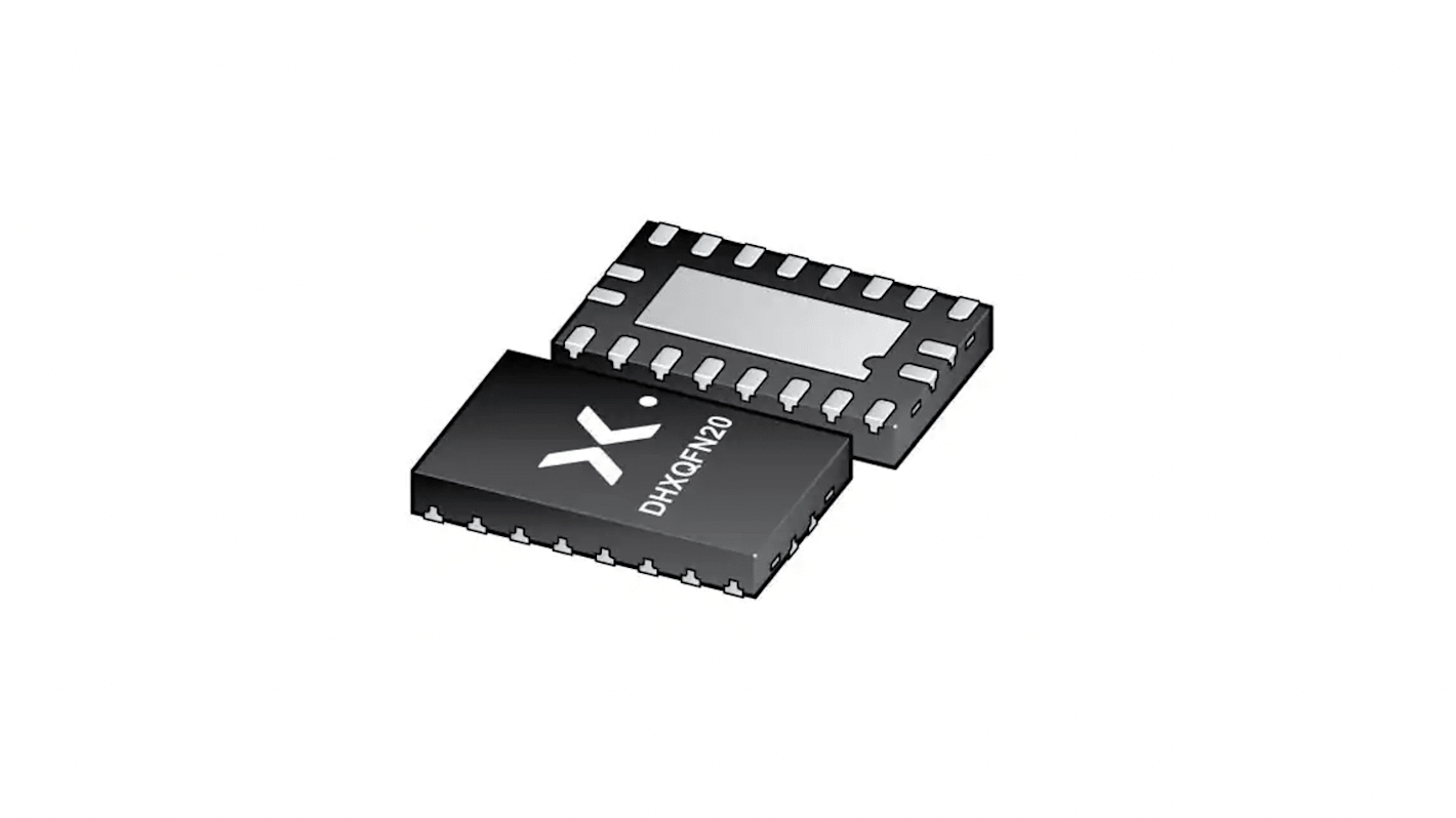
รูปภาพประกอบสินค้าเป็นเพียงรูปภาพใกล้เคียงเท่านั้น กรุณาอ่านรายละเอียดสินค้า
มีส่วนลดเมื่อซื้อจำนวนมาก
ดูตัวเลือกการกำหนดราคาในการซื้อปริมาณมากยอดรวมย่อย (1 แพ็ค แพ็คละ 25 ชิ้น)*
THB363.75
(ไม่รวมภาษีมูลค่าเพิ่ม)
THB389.25
(รวมภาษีมูลค่าเพิ่ม)
ส่งฟรีหากซื้อเกิน ฿2,500.00
มีในสต็อก
- 3,000 ชิ้นพร้อมจัดส่งจากคลังสินค้าต่างประเทศ
ต้องการสินค้าเพิ่มหรือไม่ ระบุจำนวนและคลิก ‘ตรวจสอบวันจัดส่ง’ เพื่อดูข้อมูลเพิ่มเติมเกี่ยวกับสต็อกสินค้าและการจัดส่ง
ชิ้น | ต่อหน่วย | ต่อแพ็ค* |
|---|---|---|
| 25 - 25 | THB14.55 | THB363.75 |
| 50 - 75 | THB14.114 | THB352.85 |
| 100 - 225 | THB13.549 | THB338.73 |
| 250 - 975 | THB12.871 | THB321.78 |
| 1000 + | THB12.099 | THB302.48 |
*ตัวบ่งบอกราคา / price indicative
- RS Stock No.:
- 243-4422
- หมายเลขชิ้นส่วนของผู้ผลิต / Mfr. Part No.:
- 74LVC245ABZX
- ผู้ผลิต:
- Nexperia
คุณสมบัติ / Specifications
ข้อมูลทางเทคนิค / Technical Data Sheets
Legislation and Compliance
รายละเอียดสินค้า / Product Details
ค้นหาผลิตภัณฑ์ที่คล้ายกันโดยเลือกคุณลักษณะอย่างน้อยหนึ่งรายการ
เลือกทั้งหมด | คุณลักษณะ | ค่า |
|---|---|---|
| Brand | Nexperia | |
| Product Type | Bus Transceiver | |
| Logic Family | CMOS | |
| Logic Function | Bus Transceiver | |
| Number of Channels | 18 | |
| Polarity | Non-Inverting | |
| Mount Type | Surface | |
| Package Type | SOT-8020 | |
| Minimum Supply Voltage | 1.2V | |
| Pin Count | 20 | |
| Input Level | TTL | |
| Maximum Supply Voltage | 3.6V | |
| Minimum Operating Temperature | -40°C | |
| Output Level | TTL | |
| Maximum Propagation Delay Time @ CL | 4.1ns | |
| Maximum Operating Temperature | 125°C | |
| Maximum High Level Output Current | 24mA | |
| Series | 74LVC245A | |
| Standards/Approvals | RoHS | |
| Length | 2mm | |
| Height | 0.48mm | |
| Maximum Low Level Output Current | 24mA | |
| Output Type | 3 State | |
| Automotive Standard | No | |
| เลือกทั้งหมด | ||
|---|---|---|
Brand Nexperia | ||
Product Type Bus Transceiver | ||
Logic Family CMOS | ||
Logic Function Bus Transceiver | ||
Number of Channels 18 | ||
Polarity Non-Inverting | ||
Mount Type Surface | ||
Package Type SOT-8020 | ||
Minimum Supply Voltage 1.2V | ||
Pin Count 20 | ||
Input Level TTL | ||
Maximum Supply Voltage 3.6V | ||
Minimum Operating Temperature -40°C | ||
Output Level TTL | ||
Maximum Propagation Delay Time @ CL 4.1ns | ||
Maximum Operating Temperature 125°C | ||
Maximum High Level Output Current 24mA | ||
Series 74LVC245A | ||
Standards/Approvals RoHS | ||
Length 2mm | ||
Height 0.48mm | ||
Maximum Low Level Output Current 24mA | ||
Output Type 3 State | ||
Automotive Standard No | ||
The Nexperia Octal bus transceiver with 3-state outputs features an output enable (OE) and send/receive (DIR) for direction control. A HIGH on OE causes the outputs to assume a high-impedance OFF-state. Inputs can be driven from either 3.3 V or 5 V devices. This feature allows the use of these devices as translators in mixed 3.3 V and 5 V environments. Schmitt-trigger action at all inputs makes the circuit tolerant of slower input rise and fall times. This device is fully specified for partial power down applications using IOFF. The IOFF circuitry disables the output, preventing the potentially damaging backflow current through the device when it is powered down.
Wide supply voltage range from 1.2 V to 3.6 V
CMOS low-power consumption
Direct interface with TTL levels
Overvoltage tolerant inputs to 5.5 V
Bus hold on all data inputs
IOFF circuitry provides partial Power-down mode operation
ลิงก์ที่เกี่ยวข้อง
- Nexperia Bus Transceiver 20-Pin SOT-8020
- Nexperia 74LVC245ABQ 18-Bit Non-Inverting CMOS 20-Pin DHVQFN
- onsemi 74AC245SCX Bus Transceiver 20-Pin SOIC
- onsemi 74ACT245SCX Bus Transceiver 20-Pin SOIC
- Texas Instruments SN74ALS641A-1N Bus Transceiver 20-Pin PDIP
- onsemi 74AC245MTC Bus Transceiver 20-Pin TSSOP
- Nexperia 74HC245PW 8-Bit Non-Inverting TTL, 20-Pin TSSOP
- Texas Instruments SN74ABT245BDBR Bus Transceiver 20-Pin SSOP