Infineon SRAM, CY7C1049GN-10VXI- 4 MB
- RS Stock No.:
- 182-3295
- หมายเลขชิ้นส่วนของผู้ผลิต / Mfr. Part No.:
- CY7C1049GN-10VXI
- ผู้ผลิต:
- Infineon

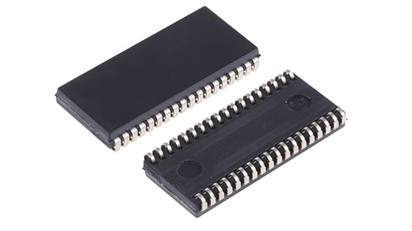
รูปภาพประกอบสินค้าเป็นเพียงรูปภาพใกล้เคียงเท่านั้น กรุณาอ่านรายละเอียดสินค้า
มีส่วนลดเมื่อซื้อจำนวนมาก
ดูตัวเลือกการกำหนดราคาในการซื้อปริมาณมากยอดรวมย่อย (1 หลอด หลอดละ 19 ชิ้น)*
THB4,410.983
(ไม่รวมภาษีมูลค่าเพิ่ม)
THB4,719.752
(รวมภาษีมูลค่าเพิ่ม)
ส่งฟรีหากซื้อเกิน ฿2,500.00
หมดสต็อกชั่วคราว
- จะส่งได้หลังจากวันที่ 18 มกราคม 2570 ไปอีกประมาณ 7 วันทำการ
ต้องการสินค้าเพิ่มหรือไม่ ระบุจำนวนและคลิก ‘ตรวจสอบวันจัดส่ง’ เพื่อดูข้อมูลเพิ่มเติมเกี่ยวกับสต็อกสินค้าและการจัดส่ง
ชิ้น | ต่อหน่วย | ต่อหลอด* |
|---|---|---|
| 19 - 19 | THB232.157 | THB4,410.98 |
| 38 - 57 | THB227.049 | THB4,313.93 |
| 76 + | THB222.174 | THB4,221.31 |
*ตัวบ่งบอกราคา / price indicative
- RS Stock No.:
- 182-3295
- หมายเลขชิ้นส่วนของผู้ผลิต / Mfr. Part No.:
- CY7C1049GN-10VXI
- ผู้ผลิต:
- Infineon
คุณสมบัติ / Specifications
ข้อมูลทางเทคนิค / Technical Data Sheets
Legislation and Compliance
รายละเอียดสินค้า / Product Details
ค้นหาผลิตภัณฑ์ที่คล้ายกันโดยเลือกคุณลักษณะอย่างน้อยหนึ่งรายการ
เลือกทั้งหมด | คุณลักษณะ | ค่า |
|---|---|---|
| Brand | Infineon | |
| Product Type | SRAM | |
| Memory Size | 4MB | |
| Organisation | 512K x 16 bit | |
| Number of Words | 512K | |
| Number of Bits per Word | 8 | |
| Maximum Random Access Time | 10ns | |
| Timing Type | Asynchronous | |
| Mount Type | Surface | |
| Package Type | SOJ | |
| Pin Count | 36 | |
| Height | 0.12mm | |
| Standards/Approvals | RoHS | |
| Width | 0.4mm | |
| Length | 0.93mm | |
| เลือกทั้งหมด | ||
|---|---|---|
Brand Infineon | ||
Product Type SRAM | ||
Memory Size 4MB | ||
Organisation 512K x 16 bit | ||
Number of Words 512K | ||
Number of Bits per Word 8 | ||
Maximum Random Access Time 10ns | ||
Timing Type Asynchronous | ||
Mount Type Surface | ||
Package Type SOJ | ||
Pin Count 36 | ||
Height 0.12mm | ||
Standards/Approvals RoHS | ||
Width 0.4mm | ||
Length 0.93mm | ||
- COO (Country of Origin):
- US
CY7C1049GN is a high-performance CMOS fast static RAM device organized as 512K words by 8-bits. Data writes are performed by asserting the Chip Enable (CE) and Write Enable (WE) inputs LOW, while providing the data on I/O0 through I/O7 and address on A0 through A18 pins. Data reads are performed by asserting the Chip Enable (CE) and Output Enable (OE) inputs LOW and providing the required address on the address lines. Read data is accessible on the I/O lines (I/O0 through I/O7). All I/Os (I/O0 through I/O7) are placed in a high-impedance state during the following events: The device is deselected (CE HIGH) The control signal OE is de-asserted.
High speed
tAA = 10 ns
Low Active and standby currents
Active current: ICC = 38 mA typical
Standby current: ISB2 = 6 mA typical
Operating voltage range: 1.65 V to 2.2 V, 2.2 V to 3.6 V, and
4.5 V to 5.5 V
1.0 V data retention
TTL-compatible inputs and outputs
Pb-free 36-pin SOJ and 44-pin TSOP II packages