Winbond W9712G6KB25I DDR2 SDRAM 128 MB Surface, 84-Pin 16 bit TFBGA
- RS Stock No.:
- 188-2730
- หมายเลขชิ้นส่วนของผู้ผลิต / Mfr. Part No.:
- W9712G6KB25I
- ผู้ผลิต:
- Winbond

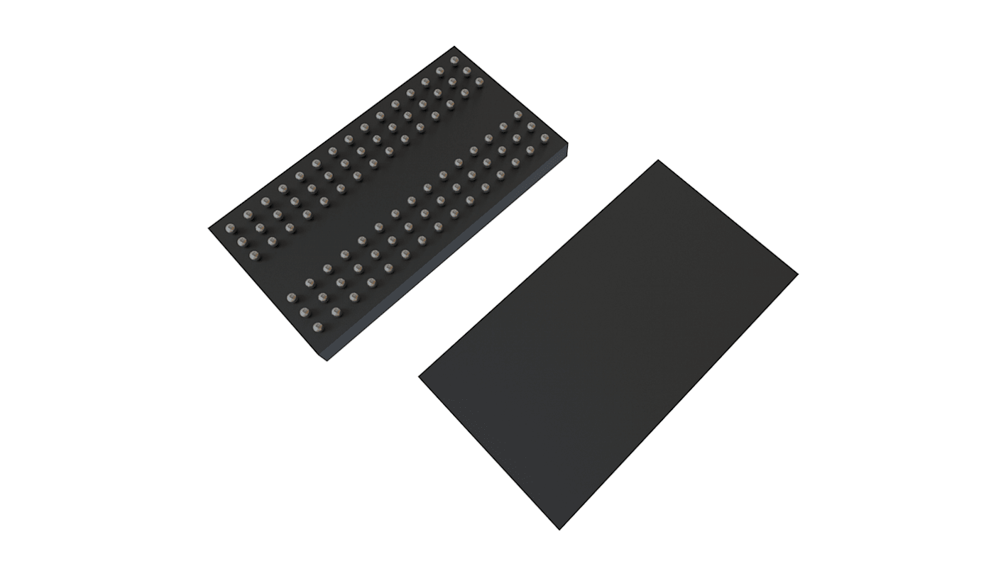
รูปภาพประกอบสินค้าเป็นเพียงรูปภาพใกล้เคียงเท่านั้น กรุณาอ่านรายละเอียดสินค้า
มีส่วนลดเมื่อซื้อจำนวนมาก
ดูตัวเลือกการกำหนดราคาในการซื้อปริมาณมากยอดรวมย่อย (1 แพ็ค แพ็คละ 5 ชิ้น)*
THB690.39
(ไม่รวมภาษีมูลค่าเพิ่ม)
THB738.715
(รวมภาษีมูลค่าเพิ่ม)
ส่งฟรีหากซื้อเกิน ฿2,500.00
หมดสต็อกชั่วคราว
- จะส่งได้หลังจากวันที่ 23 พฤศจิกายน 2569 ไปอีกประมาณ 7 วันทำการ
ต้องการสินค้าเพิ่มหรือไม่ ระบุจำนวนและคลิก ‘ตรวจสอบวันจัดส่ง’ เพื่อดูข้อมูลเพิ่มเติมเกี่ยวกับสต็อกสินค้าและการจัดส่ง
ชิ้น | ต่อหน่วย | ต่อแพ็ค* |
|---|---|---|
| 5 - 50 | THB138.078 | THB690.39 |
| 55 - 100 | THB134.626 | THB673.13 |
| 105 + | THB132.552 | THB662.76 |
*ตัวบ่งบอกราคา / price indicative
- RS Stock No.:
- 188-2730
- หมายเลขชิ้นส่วนของผู้ผลิต / Mfr. Part No.:
- W9712G6KB25I
- ผู้ผลิต:
- Winbond
คุณสมบัติ / Specifications
ข้อมูลทางเทคนิค / Technical Data Sheets
Legislation and Compliance
รายละเอียดสินค้า / Product Details
ค้นหาผลิตภัณฑ์ที่คล้ายกันโดยเลือกคุณลักษณะอย่างน้อยหนึ่งรายการ
เลือกทั้งหมด | คุณลักษณะ | ค่า |
|---|---|---|
| Brand | Winbond | |
| Memory Size | 128MB | |
| Product Type | DDR2 SDRAM | |
| Organisation | 16M x 8 bit | |
| Data Bus Width | 16bit | |
| Address Bus Width | 15bit | |
| Number of Bits per Word | 8 | |
| Maximum Random Access Time | 0.4ns | |
| Number of Words | 16M | |
| Mount Type | Surface | |
| Package Type | TFBGA | |
| Pin Count | 84 | |
| Minimum Operating Temperature | -40°C | |
| Maximum Operating Temperature | 95°C | |
| Length | 12.6mm | |
| Height | 0.8mm | |
| Standards/Approvals | RoHS | |
| Width | 8.1mm | |
| Series | W9712G6KB | |
| Maximum Supply Voltage | 1.9V | |
| Automotive Standard | No | |
| Minimum Supply Voltage | 1.7V | |
| Supply Current | 135mA | |
| เลือกทั้งหมด | ||
|---|---|---|
Brand Winbond | ||
Memory Size 128MB | ||
Product Type DDR2 SDRAM | ||
Organisation 16M x 8 bit | ||
Data Bus Width 16bit | ||
Address Bus Width 15bit | ||
Number of Bits per Word 8 | ||
Maximum Random Access Time 0.4ns | ||
Number of Words 16M | ||
Mount Type Surface | ||
Package Type TFBGA | ||
Pin Count 84 | ||
Minimum Operating Temperature -40°C | ||
Maximum Operating Temperature 95°C | ||
Length 12.6mm | ||
Height 0.8mm | ||
Standards/Approvals RoHS | ||
Width 8.1mm | ||
Series W9712G6KB | ||
Maximum Supply Voltage 1.9V | ||
Automotive Standard No | ||
Minimum Supply Voltage 1.7V | ||
Supply Current 135mA | ||
The W9712G6KB is a 128M bits DDR2 SDRAM and speed involving -25, 25I and -3.
Double Data Rate architecture: two data transfers per clock cycle
CAS Latency: 3, 4, 5 and 6
Burst Length: 4 and 8
Bi-directional, differential data strobes (DQS and /DQS ) are transmitted / received with data
Edge-aligned with Read data and center-aligned with Write data
DLL aligns DQ and DQS transitions with clock
Differential clock inputs (CLK and /CLK)
Data masks (DM) for write data
Commands entered on each positive CLK edge, data and data mask are referenced to both edges of /DQS
Posted /CAS programmable additive latency supported to make command and data bus efficiency
Read Latency = Additive Latency plus CAS Latency (RL = AL + CL)
Off-Chip-Driver impedance adjustment (OCD) and On-Die-Termination (ODT) for better signal quality
Auto-precharge operation for read and write bursts
Auto Refresh and Self Refresh modes
Precharged Power Down and Active Power Down
Write Data Mask
Write Latency = Read Latency - 1 (WL = RL - 1)
Interface: SSTL_18
ลิงก์ที่เกี่ยวข้อง
- Winbond DDR2 SDRAM 128 MB Surface, 84-Pin 16 bit TFBGA
- Micron SDRAM 128 MB Surface, 54-Pin 16 bit TSOP
- Micron MT48LC8M16A2P-6A:L SDRAM 128 MB Surface Mount, 54-Pin 16 bit TSOP
- Alliance Memory SDRAM 128 MB Surface, 54-Pin 16 bit TSOP
- Alliance Memory AS4C8M16SA-7TCN SDRAM 128 MB Surface, 54-Pin 16 bit TSOP
- Alliance Memory AS4C8M16SA-7TCNTR SDRAM 128 MB Surface, 54-Pin 16 bit TSOP
- ISSI IS43TR16128DL-107MBL-TR SDRAM 128 MB Surface, 96-Pin 16 bit BGA
- Intelligent Memory IM1216SDBABG-6I SDRAM 128 MB Surface, 54-Pin 16 bit FBGA