N-Channel MOSFET, 15 A, 500 V, 3-Pin TO-3PN onsemi FQA13N50CF
- RS Stock No.:
- 166-2164
- หมายเลขชิ้นส่วนของผู้ผลิต / Mfr. Part No.:
- FQA13N50CF
- ผู้ผลิต:
- onsemi

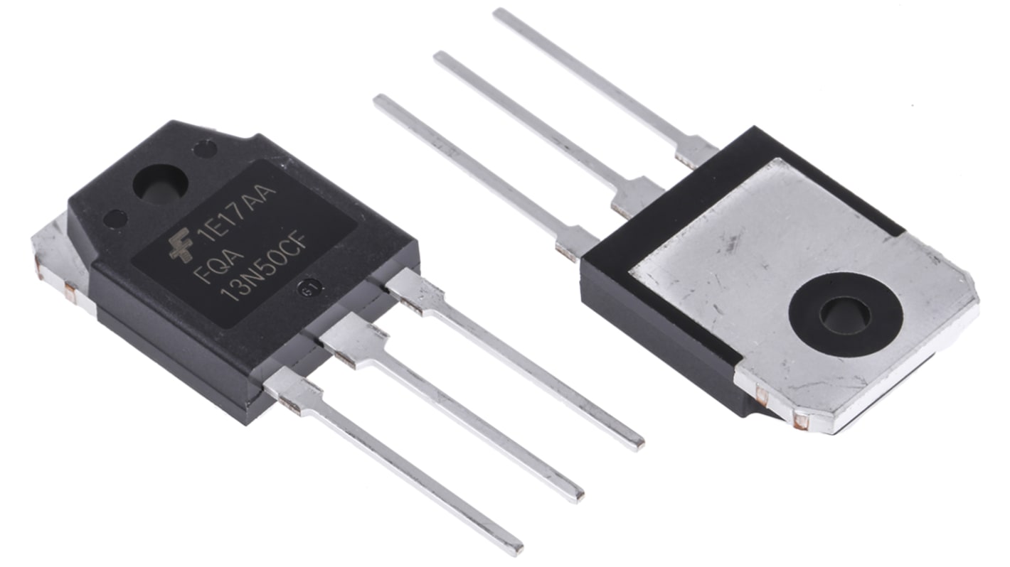
รูปภาพประกอบสินค้าเป็นเพียงรูปภาพใกล้เคียงเท่านั้น กรุณาอ่านรายละเอียดสินค้า
ไม่พร้อมจำหน่าย
RS จะไม่สต็อกสินค้านี้อีกต่อไป
- RS Stock No.:
- 166-2164
- หมายเลขชิ้นส่วนของผู้ผลิต / Mfr. Part No.:
- FQA13N50CF
- ผู้ผลิต:
- onsemi
คุณสมบัติ / Specifications
ข้อมูลทางเทคนิค / Technical Data Sheets
Legislation and Compliance
รายละเอียดสินค้า / Product Details
ค้นหาผลิตภัณฑ์ที่คล้ายกันโดยเลือกคุณลักษณะอย่างน้อยหนึ่งรายการ
เลือกทั้งหมด | คุณลักษณะ | ค่า |
|---|---|---|
| Brand | onsemi | |
| Channel Type | N | |
| Maximum Continuous Drain Current | 15 A | |
| Maximum Drain Source Voltage | 500 V | |
| Package Type | TO-3PN | |
| Mounting Type | Through Hole | |
| Pin Count | 3 | |
| Maximum Drain Source Resistance | 480 mΩ | |
| Channel Mode | Enhancement | |
| Minimum Gate Threshold Voltage | 2V | |
| Maximum Power Dissipation | 218 W | |
| Transistor Configuration | Single | |
| Maximum Gate Source Voltage | -30 V, +30 V | |
| Typical Gate Charge @ Vgs | 43 nC @ 10 V | |
| Maximum Operating Temperature | +150 °C | |
| Width | 5mm | |
| Number of Elements per Chip | 1 | |
| Transistor Material | Si | |
| Length | 15.8mm | |
| Height | 20.1mm | |
| Series | QFET | |
| Minimum Operating Temperature | -55 °C | |
| เลือกทั้งหมด | ||
|---|---|---|
Brand onsemi | ||
Channel Type N | ||
Maximum Continuous Drain Current 15 A | ||
Maximum Drain Source Voltage 500 V | ||
Package Type TO-3PN | ||
Mounting Type Through Hole | ||
Pin Count 3 | ||
Maximum Drain Source Resistance 480 mΩ | ||
Channel Mode Enhancement | ||
Minimum Gate Threshold Voltage 2V | ||
Maximum Power Dissipation 218 W | ||
Transistor Configuration Single | ||
Maximum Gate Source Voltage -30 V, +30 V | ||
Typical Gate Charge @ Vgs 43 nC @ 10 V | ||
Maximum Operating Temperature +150 °C | ||
Width 5mm | ||
Number of Elements per Chip 1 | ||
Transistor Material Si | ||
Length 15.8mm | ||
Height 20.1mm | ||
Series QFET | ||
Minimum Operating Temperature -55 °C | ||
QFET® N-Channel MOSFET, 11A to 30A, Fairchild Semiconductor
Fairchild Semiconductor’s new QFET® planar MOSFETs use advanced, proprietary technology to offer best-in-class operating performance for a wide range of applications, including power supplies, PFC (Power Factor Correction), DC-DC Converters, Plasma Display Panels (PDP), lighting ballasts, and motion control.
They offer reduced on-state loss by lowering on-resistance (RDS(on)), and reduced switching loss by lowering gate charge (Qg) and output capacitance (Coss). By using advanced QFET® process technology, Fairchild can offer an improved figure of merit (FOM) over competing planar MOSFET devices.
They offer reduced on-state loss by lowering on-resistance (RDS(on)), and reduced switching loss by lowering gate charge (Qg) and output capacitance (Coss). By using advanced QFET® process technology, Fairchild can offer an improved figure of merit (FOM) over competing planar MOSFET devices.
MOSFET Transistors, ON Semi
ON Semi offers a substantial portfolio of MOSFET devices that includes high-voltage (>250V) and low-voltage (<250V) types. The advanced silicon technology provides smaller die sizes, which it is incorporated into multiple industry-standard and thermally-enhanced packages.
ON Semi MOSFETs provide superior design reliability from reduced voltage spikes and overshoot, to lower junction capacitance and reverse recovery charge, to elimination of additional external components to keep systems up and running longer.
ON Semi MOSFETs provide superior design reliability from reduced voltage spikes and overshoot, to lower junction capacitance and reverse recovery charge, to elimination of additional external components to keep systems up and running longer.