Winbond W949D2DBJX5I, SDRAM 512Mbit Surface Mount, 200MHz, 1.7 V to 1.95 V, 90-Pin VFBGA
- RS Stock No.:
- 188-2651P
- หมายเลขชิ้นส่วนของผู้ผลิต / Mfr. Part No.:
- W949D2DBJX5I
- ผู้ผลิต:
- Winbond

ไม่พร้อมจำหน่ายในตอนนี้
เราไม่ทราบว่าสินค้านี้จะกลับมาในสต็อกหรือไม่ RS ตั้งใจที่จะลบสินค้านี้ออกจากกลุ่มผลิตภัณฑ์ในเร็วๆ นี้
- RS Stock No.:
- 188-2651P
- หมายเลขชิ้นส่วนของผู้ผลิต / Mfr. Part No.:
- W949D2DBJX5I
- ผู้ผลิต:
- Winbond
คุณสมบัติ / Specifications
ข้อมูลทางเทคนิค / Technical Data Sheets
Legislation and Compliance
รายละเอียดสินค้า / Product Details
ค้นหาผลิตภัณฑ์ที่คล้ายกันโดยเลือกคุณลักษณะอย่างน้อยหนึ่งรายการ
เลือกทั้งหมด | คุณลักษณะ | ค่า |
|---|---|---|
| Brand | Winbond | |
| Memory Size | 512Mbit | |
| SDRAM Class | LPDDR | |
| Organisation | 64M x 8 bit | |
| Data Rate | 200MHz | |
| Data Bus Width | 32bit | |
| Address Bus Width | 15bit | |
| Number of Bits per Word | 8bit | |
| Maximum Random Access Time | 5ns | |
| Number of Words | 64M | |
| Mounting Type | Surface Mount | |
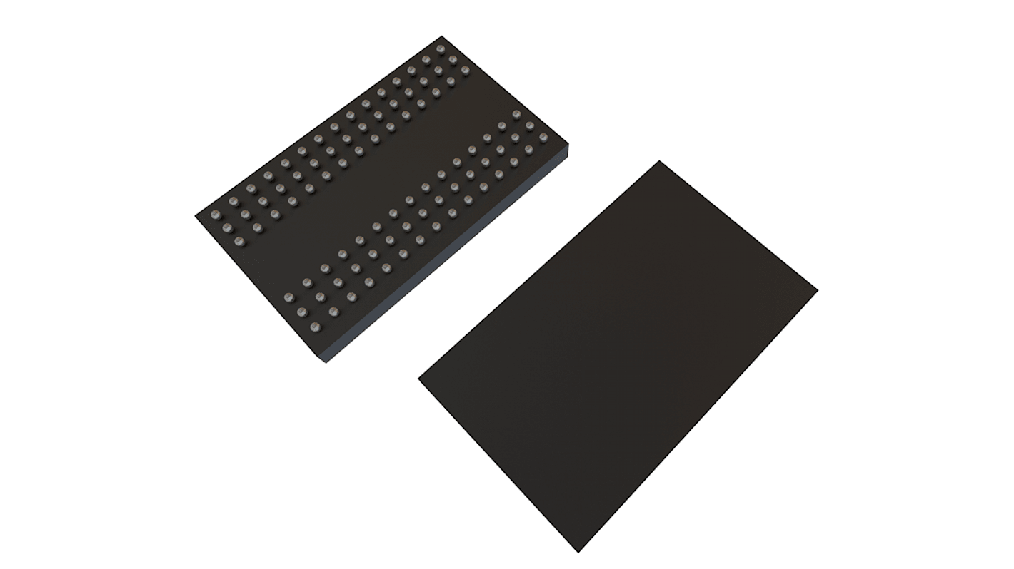
| Package Type | VFBGA | |
| Pin Count | 90 | |
| Dimensions | 13.1 x 8.1 x 0.65mm | |
| Height | 0.65mm | |
| Length | 13.1mm | |
| Minimum Operating Temperature | -40 °C | |
| Width | 8.1mm | |
| Maximum Operating Supply Voltage | 1.95 V | |
| Minimum Operating Supply Voltage | 1.7 V | |
| Maximum Operating Temperature | +85 °C | |
| เลือกทั้งหมด | ||
|---|---|---|
Brand Winbond | ||
Memory Size 512Mbit | ||
SDRAM Class LPDDR | ||
Organisation 64M x 8 bit | ||
Data Rate 200MHz | ||
Data Bus Width 32bit | ||
Address Bus Width 15bit | ||
Number of Bits per Word 8bit | ||
Maximum Random Access Time 5ns | ||
Number of Words 64M | ||
Mounting Type Surface Mount | ||
Package Type VFBGA | ||
Pin Count 90 | ||
Dimensions 13.1 x 8.1 x 0.65mm | ||
Height 0.65mm | ||
Length 13.1mm | ||
Minimum Operating Temperature -40 °C | ||
Width 8.1mm | ||
Maximum Operating Supply Voltage 1.95 V | ||
Minimum Operating Supply Voltage 1.7 V | ||
Maximum Operating Temperature +85 °C | ||
- COO (Country of Origin):
- TW
VDD = 1.7∼1.95V
VDDQ = 1.7∼1.95V
Data width: x16 / x32
Clock rate: 200MHz (-5),166MHz (-6)
Standard Self Refresh Mode
Partial Array Self-Refresh(PASR)
Auto Temperature Compensated Self Refresh (ATCSR)
Power Down Mode
Deep Power Down Mode (DPD Mode)
Programmable output buffer driver strength
Four internal banks for concurrent operation
Data mask (DM) for write data
Clock Stop capability during idle periods
Auto Pre-charge option for each burst access
Double data rate for data output
Differential clock inputs (CK and CK)
Bidirectional, data strobe (DQS)
CAS Latency: 2 and 3
Burst Length: 2, 4, 8 and 16
Burst Type: Sequential or Interleave
8K refresh cycles/64 mS
Interface: LVCMOS compatible
Support package:
60 balls VFBGA (x16)
90 balls VFBGA (x32)
Operating Temperature Range
Extended: -25°C ≤ TCASE ≤ 85°C
Industrial: -40°C ≤ TCASE ≤ 85°C
This is a 512Mb Low Power DDR SDRAM organized as 2M words x 4 banks x 32bits.
Burst Type: Sequential or Interleave
Standard Self Refresh Mode
PASR, ATCSR, Power Down Mode、DPD
Programmable output buffer driver strength
Four internal banks for concurrent operation
Bidirectional, data strobe (DQS) is transmitted or received with data, to be used in capturing data at the receiver
Standard Self Refresh Mode
PASR, ATCSR, Power Down Mode、DPD
Programmable output buffer driver strength
Four internal banks for concurrent operation
Bidirectional, data strobe (DQS) is transmitted or received with data, to be used in capturing data at the receiver