Xilinx FPGA XC3S400-5TQG144C, Spartan-3 8064 Cells, 400000 Gates, 57344bit, 8064 Blocks, 144-Pin TQFP
- RS Stock No.:
- 173-2091
- หมายเลขชิ้นส่วนของผู้ผลิต / Mfr. Part No.:
- XC3S400-5TQG144C
- ผู้ผลิต:
- Xilinx

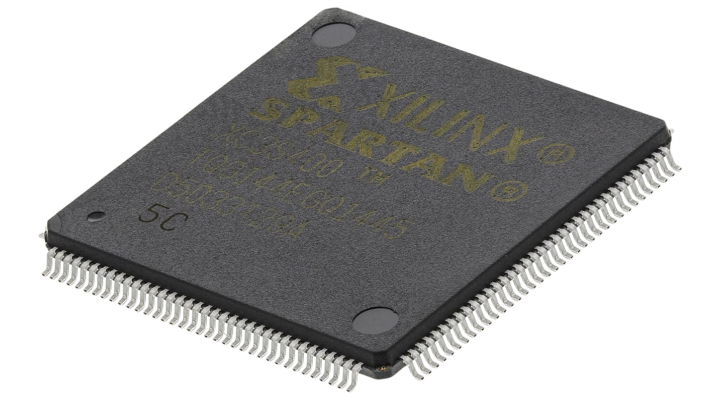
รูปภาพประกอบสินค้าเป็นเพียงรูปภาพใกล้เคียงเท่านั้น กรุณาอ่านรายละเอียดสินค้า
ไม่พร้อมจำหน่าย
RS จะไม่สต็อกสินค้านี้อีกต่อไป
- RS Stock No.:
- 173-2091
- หมายเลขชิ้นส่วนของผู้ผลิต / Mfr. Part No.:
- XC3S400-5TQG144C
- ผู้ผลิต:
- Xilinx
คุณสมบัติ / Specifications
ข้อมูลทางเทคนิค / Technical Data Sheets
Legislation and Compliance
รายละเอียดสินค้า / Product Details
ค้นหาผลิตภัณฑ์ที่คล้ายกันโดยเลือกคุณลักษณะอย่างน้อยหนึ่งรายการ
เลือกทั้งหมด | คุณลักษณะ | ค่า |
|---|---|---|
| Brand | Xilinx | |
| Family Name | Spartan-3 | |
| Number of Logic Gates | 400000 | |
| Number of Logic Cells | 8064 | |
| Number of Logic Units | 8064 | |
| Number of Multipliers | 16 (18 x 18) | |
| Mounting Type | Surface Mount | |
| Package Type | TQFP | |
| Pin Count | 144 | |
| Number of RAM Bits | 57344bit | |
| Dimensions | 20 x 20 x 1.4mm | |
| Height | 1.4mm | |
| Length | 20mm | |
| Maximum Operating Supply Voltage | 1.26 V | |
| Maximum Operating Temperature | +85 °C | |
| Width | 20mm | |
| Minimum Operating Supply Voltage | 1.14 V | |
| Minimum Operating Temperature | 0 °C | |
| เลือกทั้งหมด | ||
|---|---|---|
Brand Xilinx | ||
Family Name Spartan-3 | ||
Number of Logic Gates 400000 | ||
Number of Logic Cells 8064 | ||
Number of Logic Units 8064 | ||
Number of Multipliers 16 (18 x 18) | ||
Mounting Type Surface Mount | ||
Package Type TQFP | ||
Pin Count 144 | ||
Number of RAM Bits 57344bit | ||
Dimensions 20 x 20 x 1.4mm | ||
Height 1.4mm | ||
Length 20mm | ||
Maximum Operating Supply Voltage 1.26 V | ||
Maximum Operating Temperature +85 °C | ||
Width 20mm | ||
Minimum Operating Supply Voltage 1.14 V | ||
Minimum Operating Temperature 0 °C | ||
- COO (Country of Origin):
- KR
Field Programmable Gate Arrays, Xilinx
An FPGA is a semiconductor device consisting of a matrix of Configurable Logic Blocks (CLBs) connected through programmable interconnects. The user determines these interconnections by programming SRAM. A CLB can be simple (AND, OR gates, etc) or complex (a block of RAM). The FPGA allows changes to be made to a design even after the device is soldered into a PCB.