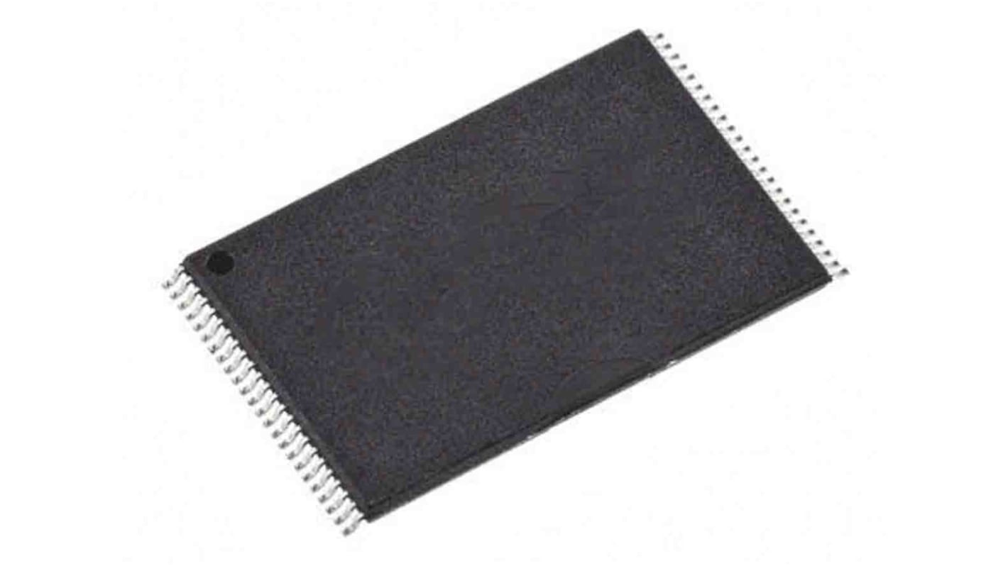
Infineon NOR 16Mbit CFI Flash Memory 48-Pin TSOP, S29AL016J70TFI013
- RS Stock No.:
- 193-8787P
- หมายเลขชิ้นส่วนของผู้ผลิต / Mfr. Part No.:
- S29AL016J70TFI013
- ผู้ผลิต:
- Infineon

มีส่วนลดเมื่อซื้อจำนวนมาก
ยอดรวมย่อย 250 ชิ้น (จัดส่งเป็นม้วน)*
THB25,203.50
(ไม่รวมภาษีมูลค่าเพิ่ม)
THB26,967.75
(รวมภาษีมูลค่าเพิ่ม)
ส่งฟรีหากซื้อเกิน ฿2,500.00
มีในสต็อก
- 985 ชิ้นพร้อมจัดส่งจากคลังสินค้าต่างประเทศ
ต้องการสินค้าเพิ่มหรือไม่ ระบุจำนวนและคลิก ‘ตรวจสอบวันจัดส่ง’ เพื่อดูข้อมูลเพิ่มเติมเกี่ยวกับสต็อกสินค้าและการจัดส่ง
ชิ้น | ต่อหน่วย |
|---|---|
| 250 - 495 | THB100.814 |
| 500 + | THB99.262 |
*ตัวบ่งบอกราคา / price indicative
- RS Stock No.:
- 193-8787P
- หมายเลขชิ้นส่วนของผู้ผลิต / Mfr. Part No.:
- S29AL016J70TFI013
- ผู้ผลิต:
- Infineon
คุณสมบัติ / Specifications
ข้อมูลทางเทคนิค / Technical Data Sheets
Legislation and Compliance
รายละเอียดสินค้า / Product Details
ค้นหาผลิตภัณฑ์ที่คล้ายกันโดยเลือกคุณลักษณะอย่างน้อยหนึ่งรายการ
เลือกทั้งหมด | คุณลักษณะ | ค่า |
|---|---|---|
| Brand | Infineon | |
| Memory Size | 16Mbit | |
| Interface Type | CFI | |
| Package Type | TSOP | |
| Pin Count | 48 | |
| Organisation | 2M x 8 bit | |
| Mounting Type | Surface Mount | |
| Cell Type | NOR | |
| Minimum Operating Supply Voltage | 2.7 V | |
| Maximum Operating Supply Voltage | 3.6 V | |
| Block Organisation | Asymmetrical | |
| Length | 12mm | |
| Height | 1.05mm | |
| Width | 18.4mm | |
| Dimensions | 18.4 x 12 x 1.05mm | |
| Series | S29AL | |
| Automotive Standard | AEC-Q100 | |
| Number of Bits per Word | 8bit | |
| Minimum Operating Temperature | -40 °C | |
| Maximum Operating Temperature | +85 °C | |
| Number of Words | 2M | |
| Maximum Random Access Time | 70ns | |
| เลือกทั้งหมด | ||
|---|---|---|
Brand Infineon | ||
Memory Size 16Mbit | ||
Interface Type CFI | ||
Package Type TSOP | ||
Pin Count 48 | ||
Organisation 2M x 8 bit | ||
Mounting Type Surface Mount | ||
Cell Type NOR | ||
Minimum Operating Supply Voltage 2.7 V | ||
Maximum Operating Supply Voltage 3.6 V | ||
Block Organisation Asymmetrical | ||
Length 12mm | ||
Height 1.05mm | ||
Width 18.4mm | ||
Dimensions 18.4 x 12 x 1.05mm | ||
Series S29AL | ||
Automotive Standard AEC-Q100 | ||
Number of Bits per Word 8bit | ||
Minimum Operating Temperature -40 °C | ||
Maximum Operating Temperature +85 °C | ||
Number of Words 2M | ||
Maximum Random Access Time 70ns | ||
The S29AL016J is a 16 Mbit, 3.0 Volt-only Flash memory organized as 2,097,152 bytes or 1,048,576 words. The device is offered in 48-ball Fine-pitch BGA (0.8 mm pitch), 64-ball Fortified BGA (1.0 mm pitch) and 48pin TSOP packages. The word-wide data (x16)appears on DQ15–DQ0, the byte-wide (x8) data appears on DQ7–DQ0. This device is designed to be programmed in-system with the standard system 3.0 volt VCC supply. A 12.0 V VPP or 5.0 VCC are not required for write or erase operations. The device can also be programmed in standard EPROM programmers.
The device offers access time of 55 ns allowing high speed microprocessors to operate without wait states. To eliminate bus contention the device has separate chip enable (CE#), write enable (WE#) and output enable (OE#) controls.
Device programming occurs by executing the program command sequence. This initiates the Embedded Program algorithm an internal algorithm that automatically times the program pulse widths and verifies proper cell margin. The Unlock Bypass mode facilitates faster programming times by requiring only two write cycles to program data instead of four.
Device erasure occurs by executing the erase command sequence. This initiates the Embedded Erase algorithm an internal algorithm that automatically preprograms the array (if it is not already programmed) before executing the erase operation. During erase, the device automatically times the erase pulse widths and verifies proper cell margin. The host system can detect whether a program or erase operation is complete by observing the RY/BY# pin, or by reading the DQ7(Data# Polling) and DQ6 (toggle) status bits. After a program or erase cycle has been completed, the device is ready to read array data or accept another command.