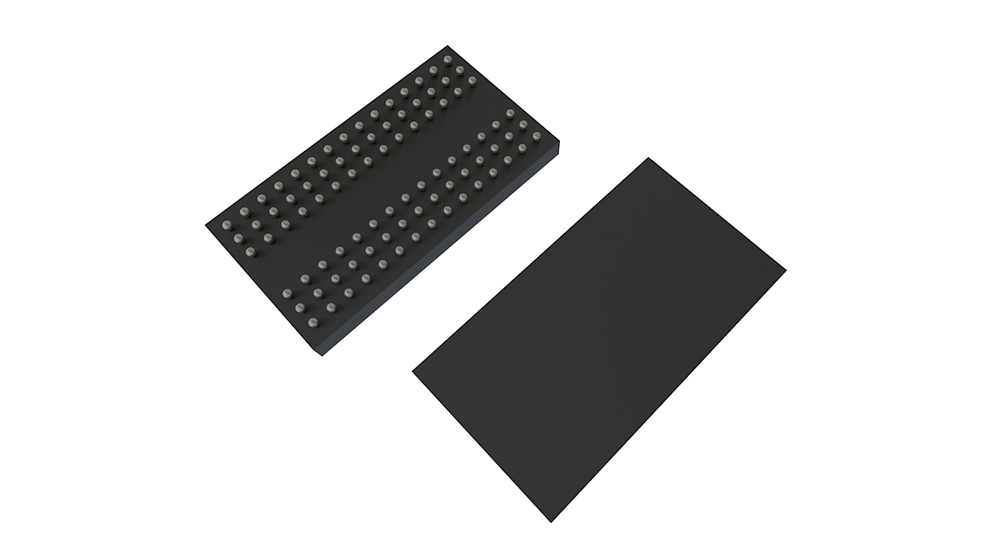
Winbond W971GG8SB25I, SDRAM 1Gbit Surface Mount, 60-Pin WBGA

- RS Stock No.:
- 188-2782P
- หมายเลขชิ้นส่วนของผู้ผลิต / Mfr. Part No.:
- W971GG8SB25I
- ผู้ผลิต / Manufacturer:
- Winbond
ผลิตภัณฑ์ที่เลิกผลิตแล้ว
- RS Stock No.:
- 188-2782P
- หมายเลขชิ้นส่วนของผู้ผลิต / Mfr. Part No.:
- W971GG8SB25I
- ผู้ผลิต / Manufacturer:
- Winbond
ข้อมูลทางเทคนิค / Technical Data Sheets
Legislation and Compliance
- COO (Country of Origin):
- TW
รายละเอียดสินค้า / Product Details
Power Supply: VDD, VDDQ = 1.8 V ± 0.1 V
Double Data Rate architecture: two data transfers per clock cycle
CAS Latency: 3, 4, 5, 6 and 7
Burst Length: 4 and 8
Bi-directional, differential data strobes (DQS and DQS) are transmitted / received with data
Edge-aligned with Read data and center-aligned with Write data
DLL aligns DQ and DQS transitions with clock
Differential clock inputs (CLK and CLK)
Data masks (DM) for write data
Commands entered on each positive CLK edge, data and data mask are referenced to both edges of DQS
Posted CAS programmable additive latency supported to make command and data bus efficiency
Read Latency = Additive Latency plus CAS Latency (RL = AL + CL)
Off-Chip-Driver impedance adjustment (OCD) and On-Die-Termination (ODT) for better signal quality
Auto-precharge operation for read and write bursts
Auto Refresh and Self Refresh modes
Precharged Power Down and Active Power Down
Write Data Mask
Write Latency = Read Latency - 1 (WL = RL - 1)
Interface: SSTL_18
Packaged in WBGA 60 Ball (8x12.5 mm2), using Lead free materials.
คุณสมบัติ / Specifications
คุณสมบัติ | Value |
|---|---|
| Memory Size | 1Gbit |
| Organisation | 128M x 8 bit |
| Number of Bits per Word | 8bit |
| Number of Words | 128M |
| Mounting Type | Surface Mount |
| Package Type | WBGA |
| Pin Count | 60 |
| Dimensions | 12.6 x 8.1 x 0.6mm |
| Height | 0.6mm |
| Length | 12.6mm |
| Minimum Operating Temperature | -40 °C |
| Maximum Operating Supply Voltage | 1.9 V |
| Minimum Operating Supply Voltage | 1.7 V |
| Width | 8.1mm |
| Maximum Operating Temperature | +95 °C |