Skyworks Solutions Inc Si53119-EK, Clock Buffer Evaluation Board for Si53119

- RS Stock No.:
- 865-1439
- หมายเลขชิ้นส่วนของผู้ผลิต / Mfr. Part No.:
- Si53119-EK
- ผู้ผลิต / Manufacturer:
- Skyworks Solutions Inc
ผลิตภัณฑ์ที่เลิกผลิตแล้ว
- RS Stock No.:
- 865-1439
- หมายเลขชิ้นส่วนของผู้ผลิต / Mfr. Part No.:
- Si53119-EK
- ผู้ผลิต / Manufacturer:
- Skyworks Solutions Inc
ข้อมูลทางเทคนิค / Technical Data Sheets
Legislation and Compliance
รายละเอียดสินค้า / Product Details
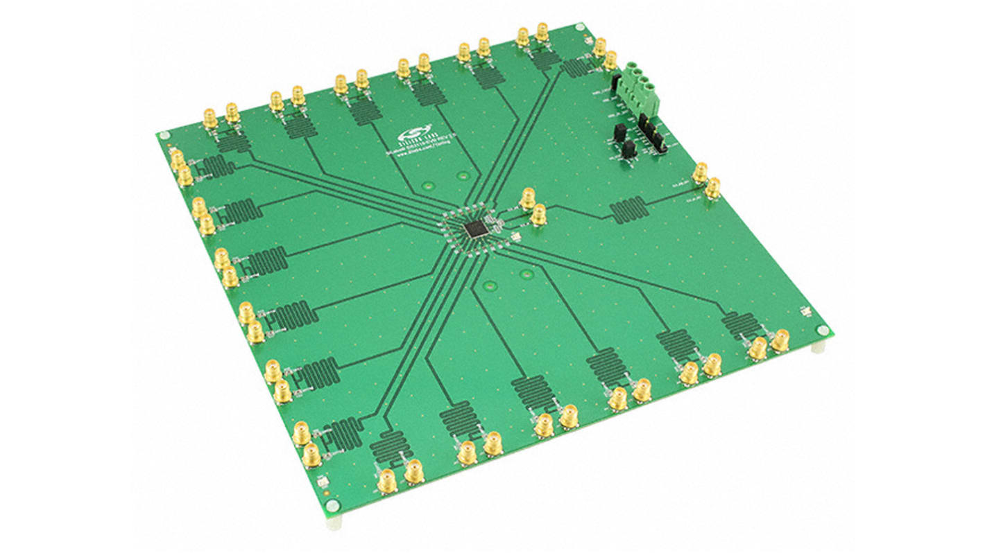
Evaluation board for Si53119, 19 Output PCIe Clock Buffer, Silicon Laboratories
The Si53119-EK by Silicon Laboratories is a PCIe clock & development kit that offers a high performance level per watt for clocking applications necessary to meet PCI Express® Gen1/2/3 standards. These clock generators and buffers have two times lower power and are able to provide up to 50% margin to PCI-Express jitter specifications. Silicon Labs Si53119-EK PCIe Clock Generators and Buffers fully integrate termination resistors, reduce BOM cost, board space requirements and design complexity.
The Si53119 is a 19-output, low-power HCSL differential clock buffer that meets all of the performance requirements of the Intel DB1200ZL specification.
The Si53119 is a 19-output, low-power HCSL differential clock buffer that meets all of the performance requirements of the Intel DB1200ZL specification.
Nineteen 0.7 V low-power, pushpull HCSL PCIe Gen 3 outputs
100 MHz /133 MHz PLL operation, supports PCIe and QPI
PLL bandwidth SW SMBUS programming overrides the latch value from HW pin
9 selectable SMBUS addresses
SMBus address configurable to allow multiple buffers in a single control network 3.3 V supply voltage operation
Separate VDDIO for outputs
PLL or bypass mode
Spread spectrum tolerable
1.05 to 3.3 V I/O supply voltage
50 ps output-to-output skew
50 ps cyc-cyc jitter (PLL mode)
Low phase jitter (Intel® QPI, PCIe Gen 1/Gen 2/Gen 3 compliant)
100 ps input-to-output delay
Extended Temperature: –40 to 85 °C
72-pin QFN
For products that are Customized and under Non-cancellable & Non-returnable, Sales & Conditions apply.
คุณสมบัติ / Specifications
คุณสมบัติ | Value |
|---|---|
| Clock/Timer Function | Clock Buffer |
| Kit Classification | Evaluation Board |
| Featured Device | Si53119 |